JAJSCD8C August 2015 – May 2017 LP8861-Q1
PRODUCTION DATA.
- 1 特長
- 2 アプリケーション
- 3 概要
- 4 改訂履歴
- 5 デバイス比較表
- 6 Pin Configuration and Functions
-
7 Specifications
- 7.1 Absolute Maximum Ratings
- 7.2 ESD Ratings
- 7.3 Recommended Operating Conditions
- 7.4 Thermal Information
- 7.5 Electrical Characteristics
- 7.6 Internal LDO Electrical Characteristics
- 7.7 Protection Electrical Characteristics
- 7.8 Power Line FET Control Electrical Characteristics
- 7.9 Current Sinks Electrical Characteristics
- 7.10 PWM Brightness Control Electrical Characteristics
- 7.11 Boost/SEPIC Converter Characteristics
- 7.12 Logic Interface Characteristics
- 7.13 Typical Characteristics
-
8 Detailed Description
- 8.1 Overview
- 8.2 Functional Block Diagram
- 8.3 Feature Description
- 8.4 Device Functional Modes
-
9 Application and Implementation
- 9.1 Application Information
- 9.2 Typical Applications
- 10Power Supply Recommendations
- 11Layout
- 12デバイスおよびドキュメントのサポート
- 13メカニカル、パッケージ、および注文情報
パッケージ・オプション
メカニカル・データ(パッケージ|ピン)
- PWP|20
サーマルパッド・メカニカル・データ
- PWP|20
発注情報
8.4.1 Device States
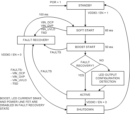
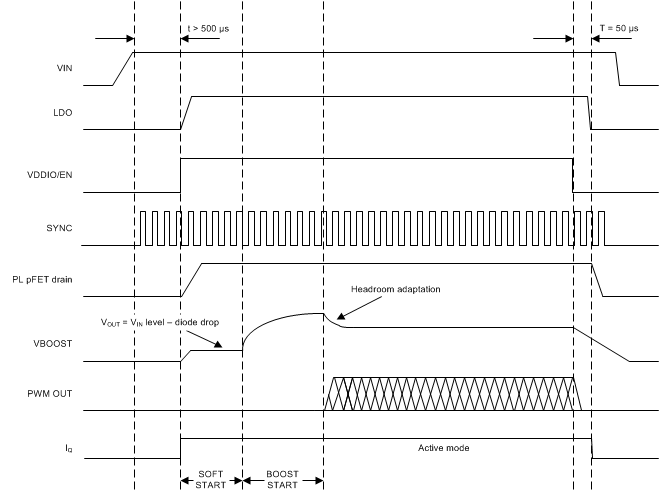
The LP8861-Q1 enters STANDBY mode when the internal LDO output rises above the power-on reset level, VLDO > VPOR_R. In STANDBY mode device is able to detect the VDDIO/EN signal. When VDDIO/EN is pulled high, device powers up. During soft start the external power line FET is opened gradually to limit inrush current. Soft start is followed by boost start, during which time boost voltage is ramped to the initial value. After boost start LED outputs are sensed to detect grounded current sinks. Grounded current sinks are disabled and excluded from the boost voltage control loop.
If a fault condition is detected, the LP8861-Q1 enters FAULT_RECOVERY state. In this state power line FET is switched off and both the boost and LED current sinks are disabled. Fault that cause the device to enter FAULT_RECOVERY are listed in Figure 22. When LED open or short is detected, faulty string is disabled but LP8861-Q1 stays in ACTIVE mode.
 Figure 22. State Diagram
  Figure 23. Timing Diagram for the Typical Start-Up and Shutdown