JAJSHS3 August   2019 LP8867C-Q1 , LP8869C-Q1

PRODUCTION DATA.  

  1. 特長
    1.     概略回路図
  2. アプリケーション
  3. 概要
    1.     システム効率
  4. 改訂履歴
  5. Device Comparison Table
  6. Pin Configuration and Functions
    1.     Pin Functions
  7. Specifications
    1. 7.1  Absolute Maximum Ratings
    2. 7.2  ESD Ratings
    3. 7.3  Recommended Operating Conditions
    4. 7.4  Thermal Information
    5. 7.5  Electrical Characteristics
    6. 7.6  Internal LDO Electrical Characteristics
    7. 7.7  Protection Electrical Characteristics
    8. 7.8  Current Sinks Electrical Characteristics
    9. 7.9  PWM Brightness Control Electrical Characteristics
    10. 7.10 Boost and SEPIC Converter Characteristics
    11. 7.11 Logic Interface Characteristics
    12. 7.12 Typical Characteristics
  8. Detailed Description
    1. 8.1 Overview
    2. 8.2 Functional Block Diagram
    3. 8.3 Feature Description
      1. 8.3.1 Integrated DC-DC Converter
        1. 8.3.1.1 DC-DC Converter Parameter Configuration
          1. 8.3.1.1.1 Switching Frequency
          2. 8.3.1.1.2 Spread Spectrum and External SYNC
          3. 8.3.1.1.3 Recommended Component Value and Internal Parameters
          4. 8.3.1.1.4 DC-DC Converter Switching Current Limit
          5. 8.3.1.1.5 DC-DC Converter Light Load Mode
        2. 8.3.1.2 Adaptive Voltage Control
          1. 8.3.1.2.1 Using Two-Divider
          2. 8.3.1.2.2 Using T-Divider
          3. 8.3.1.2.3 Feedback Capacitor
      2. 8.3.2 Internal LDO
      3. 8.3.3 LED Current Sinks
        1. 8.3.3.1 LED Output Configuration
        2. 8.3.3.2 LED Current Setting
        3. 8.3.3.3 Brightness Control
      4. 8.3.4 Protection and Fault Detections
        1. 8.3.4.1 Supply Fault and Protection
          1. 8.3.4.1.1 VIN Undervoltage Fault (VIN_UVLO)
          2. 8.3.4.1.2 VIN Overvoltage Fault (VIN_OVP)
        2. 8.3.4.2 Boost Fault and Protection
          1. 8.3.4.2.1 Boost Overvoltage Fault (BST_OVP)
          2. 8.3.4.2.2 SW Overvoltage Fault (SW_OVP)
        3. 8.3.4.3 LED Fault and Protection
          1. 8.3.4.3.1 LED Open Fault (LED_OPEN)
          2. 8.3.4.3.2 LED Short Fault (LED_SHORT)
        4. 8.3.4.4 Thermal Fault and Protection (TSD)
        5. 8.3.4.5 Overview of the Fault and Protection Schemes
    4. 8.4 Device Functional Modes
      1. 8.4.1 STANDBY State
      2. 8.4.2 SOFT START State
      3. 8.4.3 BOOST START State
      4. 8.4.4 NORMAL State
      5. 8.4.5 FAULT RECOVERY State
      6. 8.4.6 State Diagram and Timing Diagram for Start-up and Shutdown
  9. Application and Implementation
    1. 9.1 Application Information
    2. 9.2 Typical Applications
      1. 9.2.1 Typical Application for 4 LED Strings
        1. 9.2.1.1 Design Requirements
        2. 9.2.1.2 Detailed Design Procedure
          1. 9.2.1.2.1 Inductor Selection
          2. 9.2.1.2.2 Output Capacitor Selection
          3. 9.2.1.2.3 Input Capacitor Selection
          4. 9.2.1.2.4 LDO Output Capacitor
          5. 9.2.1.2.5 Diode
        3. 9.2.1.3 Application Curves
      2. 9.2.2 SEPIC Mode Application
        1. 9.2.2.1 Design Requirements
        2. 9.2.2.2 Detailed Design Procedure
          1. 9.2.2.2.1 Inductor
          2. 9.2.2.2.2 Diode
          3. 9.2.2.2.3 Capacitor C1
        3. 9.2.2.3 Application Curves
  10. 10Power Supply Recommendations
  11. 11Layout
    1. 11.1 Layout Guidelines
    2. 11.2 Layout Example
  12. 12デバイスおよびドキュメントのサポート
    1. 12.1 デバイス・サポート
      1. 12.1.1 開発サポート
    2. 12.2 ドキュメントのサポート
      1. 12.2.1 関連資料
    3. 12.3 ドキュメントの更新通知を受け取る方法
    4. 12.4 コミュニティ・リソース
    5. 12.5 商標
    6. 12.6 静電気放電に関する注意事項
    7. 12.7 Glossary
  13. 13メカニカル、パッケージ、および注文情報

パッケージ・オプション

メカニカル・データ(パッケージ|ピン)
サーマルパッド・メカニカル・データ
発注情報

Using T-Divider

Alternatively, a T-divider can be used if resistance less than 100 kΩ is required for the external resistive divider. Then the maximum, minimum and initial boost voltages can be calculated with

Equation 3. LP8867C-Q1 LP8869C-Q1 eq-01-adaptive-Tres.gif

where

  • VBG = 1.2 V
  • R2 recommended value is 10 kΩ to 200 kΩ
  • R1/R2 recommended value is 5 to 10 for <1150kHz DC-DC switching frequency
  • R1/R2 recommended value is 10 to 20 for >1150kHz DC-DC switching frequency
  • K = 1 for maximum adaptive boost voltage (typical)
  • K = 0 for minimum adaptive boost voltage (typical)
  • K = 0.88 for initial boost voltage (typical)

For example, if R1 is set to 100 kΩ, R2 is set to 10 kΩ and R3 is set to 60 kΩ, VBOOST will be in the range of 13.2 V to 42.6 V.
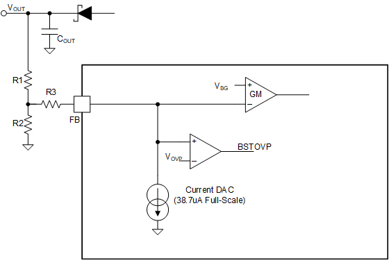
LP8867C-Q1 LP8869C-Q1 fb-03-fb_Tres.gifFigure 12. FB external T-divider resistors