JAJSHN1A June 2019 – August 2019 LP8867-Q1 , LP8869-Q1
PRODUCTION DATA.
- 1 特長
- 2 アプリケーション
- 3 概要
- 4 改訂履歴
- 5 概要 (続き)
- 6 Device Comparison Table
- 7 Pin Configuration and Functions
-
8 Specifications
- 8.1 Absolute Maximum Ratings
- 8.2 ESD Ratings
- 8.3 Recommended Operating Conditions
- 8.4 Thermal Information
- 8.5 Electrical Characteristics
- 8.6 Internal LDO Electrical Characteristics
- 8.7 Protection Electrical Characteristics
- 8.8 Current Sinks Electrical Characteristics
- 8.9 PWM Brightness Control Electrical Characteristics
- 8.10 Boost and SEPIC Converter Characteristics
- 8.11 Logic Interface Characteristics
- 8.12 Typical Characteristics
-
9 Detailed Description
- 9.1 Overview
- 9.2 Functional Block Diagram
- 9.3
Feature Description
- 9.3.1 Integrated DC-DC Converter
- 9.3.2 Internal LDO
- 9.3.3 LED Current Sinks
- 9.3.4 Power-Line FET Control
- 9.3.5 LED Current Dimming With External Temperature Sensor
- 9.3.6 Fault Detections and Protection
- 9.4 Device Functional Modes
- 10Application and Implementation
- 11Power Supply Recommendations
- 12Layout
- 13デバイスおよびドキュメントのサポート
- 14メカニカル、パッケージ、および注文情報
パッケージ・オプション
メカニカル・データ(パッケージ|ピン)
- PWP|20
サーマルパッド・メカニカル・データ
- PWP|20
発注情報
9.3.6.3 LED Fault and Protection (LED_OPEN and LED_SHORT)
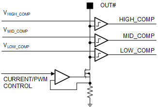
Every LED current sink has 3 comparators for LED fault detections.
 Figure 18. Comparators for LED Fault Detection
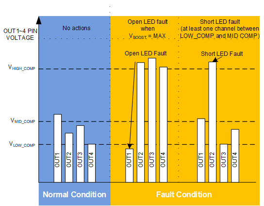
 Figure 19 shows cases which generates LED faults. Any LED faults will pull the Fault pin low.
During normal operation, boost voltage is raised if any of the used LED outputs falls below the VLOW_COMP threshold. Open LED fault is detected if boost output voltage has reached the maximum and at least one LED output is still below the threshold. The open string is then disconnected from the boost adaptive control loop and its output is disabled.
Shorted LED fault is detected if one or more LED outputs are above the VHIGH_COMP threshold (typical 6 V) and at least one LED output is inside the normal operation window (between VLOW_COMP and VMID_COMP, typical 0.9 V and 1.9 V). The shorted string is disconnected from the boost adaptive control loop and its output is disabled.
LED Open fault detection and LED Short fault detection are available only in NORMAL state.
 Figure 19. Protection and DC-DC Voltage Adaptation Algorithms
 If LED fault is detected, the device continues normal operation and only the faulty string is disabled. The fault is indicated via the FAULT pin which can be released by toggling VDDIO/EN pin low for a short period of 2 µs to 20 µs. LEDs are turned off for this period but the device stays in NORMAL state. If VDDIO/EN is low longer, the device goes to STANDBY and restarts when EN goes high again.
This means if the system doesn't want to simply disable the device because of LED faults. It could clear the LED faults by toggling VDDIO/EN pin low for a short period of 2 µs to 20 µs.