JAJSS82E August 2009 – July 2024 LPV521
PRODUCTION DATA
- 1
- 1 特長
- 2 アプリケーション
- 3 概要
- 4 Pin Configuration and Functions
- 5 Specifications
- 6 Detailed Description
- 7 Applications and Implementation
- 8 Device and Documentation Support
- 9 Revision History
- 10Mechanical, Packaging, and Orderable Information
パッケージ・オプション
メカニカル・データ(パッケージ|ピン)
サーマルパッド・メカニカル・データ
発注情報
5.6 Typical Characteristics
at TJ = 25°C (unless otherwise specified)
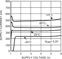 Figure 5-1 Supply Current vs Supply Voltage
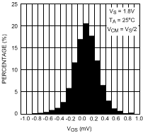 Figure 5-3 Offset Voltage Distribution
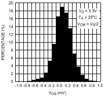 Figure 5-5 Offset Voltage Distribution
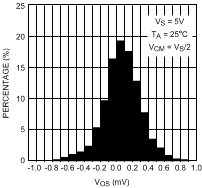 Figure 5-7 Offset Voltage Distribution
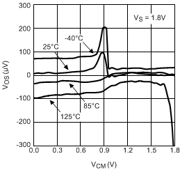 Figure 5-9 Input Offset Voltage vs Input Common
Mode
 Figure 5-11 Input Offset Voltage vs Input Common
Mode
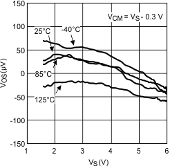 Figure 5-13 Input Offset Voltage vs Supply Voltage
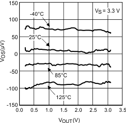 Figure 5-15 Input Offset Voltage vs Output Voltage
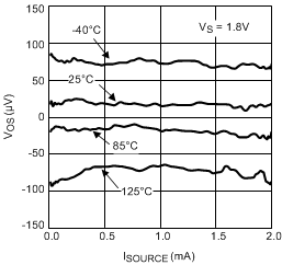 Figure 5-17 Input Offset Voltage vs Sourcing
Current
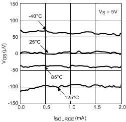 Figure 5-19 Input Offset Voltage vs Sourcing
Current
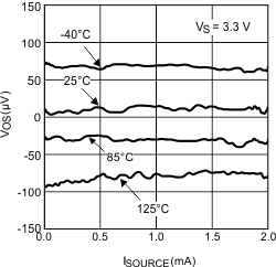 Figure 5-21 Input Offset Voltage vs Sinking
Current
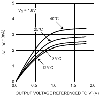 Figure 5-23 Sourcing Current vs Output Voltage
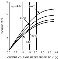 Figure 5-25 Sourcing Current vs Output Voltage
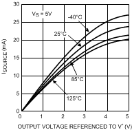 Figure 5-27 Sourcing Current vs Output Voltage
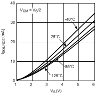 Figure 5-29 Sourcing Current vs Supply Voltage
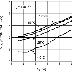 Figure 5-31 Output Swing High vs Supply Voltage
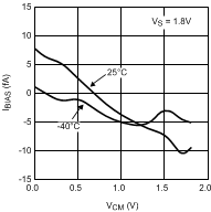 Figure 5-33 Input Bias Current vs Common Mode
Voltage
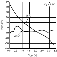 Figure 5-35 Input Bias Current vs Common Mode
Voltage
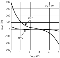 Figure 5-37 Input Bias Current vs Common Mode
Voltage
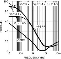 Figure 5-39 PSRR vs Frequency
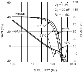 Figure 5-41 Frequency Response vs Temperature
 Figure 5-43 Frequency Response vs Temperature
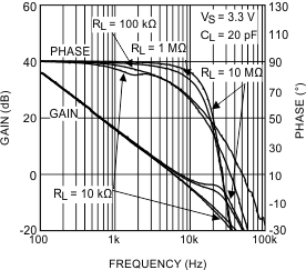 Figure 5-45 Frequency Response vs RL
 Figure 5-47 Frequency Response vs CL
 Figure 5-49 Frequency Response vs CL
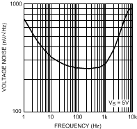 Figure 5-51 Voltage Noise vs Frequency
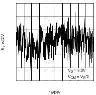 Figure 5-53 0.1-Hz to 10-Hz Time Domain Voltage
Noise
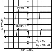 Figure 5-55 Small-Signal Pulse Response
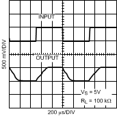 Figure 5-57 Large-Signal Pulse Response
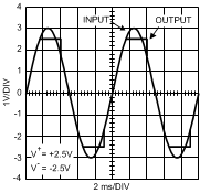
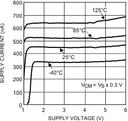 Figure 5-2 Supply Current vs Supply Voltage
 Figure 5-4 TcvOS Distribution
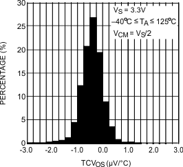 Figure 5-6 TcvOS Distribution
 Figure 5-8 TcvOS Distribution
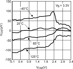 Figure 5-10 Input Offset Voltage vs Input Common
Mode
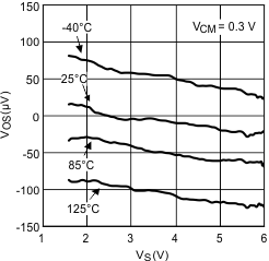 Figure 5-12 Input Offset Voltage vs Supply Voltage
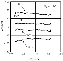 Figure 5-14 Input Offset Voltage vs Output Voltage
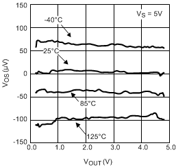 Figure 5-16 Input Offset Voltage vs Output Voltage
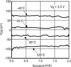 Figure 5-18 Input Offset Voltage vs Sourcing
Current
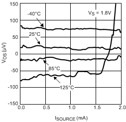 Figure 5-20 Input Offset Voltage vs Sinking
Current
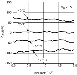 Figure 5-22 Input Offset Voltage vs Sinking
Current
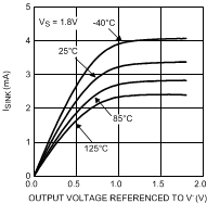 Figure 5-24 Sinking Current vs Output Voltage
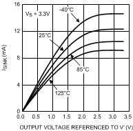 Figure 5-26 Sinking Current vs Output Voltage
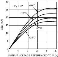 Figure 5-28 Sinking Current vs Output Voltage
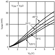 Figure 5-30 Sinking Current vs Supply Voltage
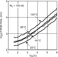 Figure 5-32 Output Swing Low vs Supply Voltage
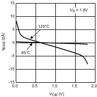 Figure 5-34 Input Bias Current vs Common Mode
Voltage
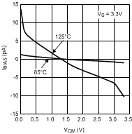 Figure 5-36 Input Bias Current vs Common Mode
Voltage
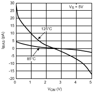 Figure 5-38 Input Bias Current vs Common Mode
Voltage
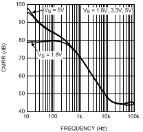 Figure 5-40 CMRR vs Frequency
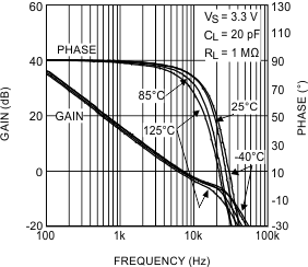 Figure 5-42 Frequency Response vs Temperature
 Figure 5-44 Frequency Response vs RL
 Figure 5-46 Frequency Response vs RL
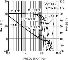 Figure 5-48 Frequency Response vs CL
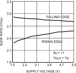 Figure 5-50 Slew Rate vs Supply Voltage
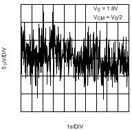 Figure 5-52 0.1-Hz to 10-Hz Time Domain Voltage
Noise
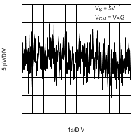 Figure 5-54 0.1-Hz to 10-Hz Time Domain Voltage
Noise
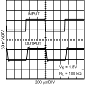 Figure 5-56 Small-Signal Pulse Response
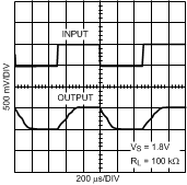 Figure 5-58 Large-Signal Pulse Response
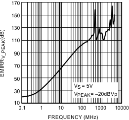 Figure 5-60 EMIRR vs Frequency