JAJSS82E August 2009 – July 2024 LPV521
PRODUCTION DATA
- 1
- 1 特長
- 2 アプリケーション
- 3 概要
- 4 Pin Configuration and Functions
- 5 Specifications
- 6 Detailed Description
- 7 Applications and Implementation
- 8 Device and Documentation Support
- 9 Revision History
- 10Mechanical, Packaging, and Orderable Information
パッケージ・オプション
メカニカル・データ(パッケージ|ピン)
サーマルパッド・メカニカル・データ
発注情報
7.1.1 Driving Capacitive Load
The LPV521 is internally compensated for stable unity gain operation, with a 6.2kHz, typical gain bandwidth. However, the unity gain follower is the most sensitive configuration to capacitive load. The combination of a capacitive load placed at the output of an amplifier along with the amplifier output impedance creates a phase lag, which reduces the phase margin of the amplifier. If the phase margin is significantly reduced, the response is underdamped, and causes peaking in the transfer. When there is too much peaking, the op amp can start oscillating.
 Figure 7-1 Resistive Isolation of Capacitive Load
To drive heavy capacitive loads, use an isolation resistor, RISO, as in Figure 7-1. By using this isolation resistor, the capacitive load is isolated from the amplifier output. The larger the value of RISO, the more stable the amplifier. If the value of RISO is sufficiently large, the feedback loop is stable, independent of the value of CL. However, larger values of RISO result in reduced output swing and reduced output current drive.
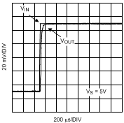
Table 7-1 shows the recommended minimum RISO values for a 5V supply. Figure 7-2 shows the typical response obtained with the CL = 50pF and RISO = 154kΩ. The other values of RISO in Table 7-1 are chosen to achieve similar dampening at the respective capacitive loads. Notice that for the LPV521 with larger a CL, a smaller RISO can be used for stability. However, for a given CL, a larger RISO provides a more damped response. For capacitive loads of 20pF and less, no isolation resistor is needed.
| CL | RISO |
|---|---|
| 0pF to 20pF | Not needed |
| 50pF | 154kΩ |
| 100pF | 118kΩ |
| 500pF | 52.3kΩ |
| 1nF | 33.2kΩ |
| 5nF | 17.4kΩ |
| 10nF | 13.3kΩ |
 Figure 7-2 Step Response