JAJSA95J September 2005 – August 2016 LPV7215
PRODUCTION DATA.
- 1 特長
- 2 アプリケーション
- 3 概要
- 4 改訂履歴
- 5 Pin Configuration and Functions
- 6 Specifications
- 7 Detailed Description
- 8 Application and Implementation
- 9 Power Supply Recommendations
- 10Layout
- 11デバイスおよびドキュメントのサポート
- 12メカニカル、パッケージ、および注文情報
パッケージ・オプション
メカニカル・データ(パッケージ|ピン)
サーマルパッド・メカニカル・データ
発注情報
7 Detailed Description
7.1 Overview
The LPV7215 is a single-channel comparator with a push-pull output stage. This comparator is optimized for low-power consumption and single-supply operation with greater than rail-to-rail input operation. The push-pull output of the LPV7215 supports rail-to-rail output swing and interfaces with TTL/CMOS logic.
7.2 Functional Block Diagram
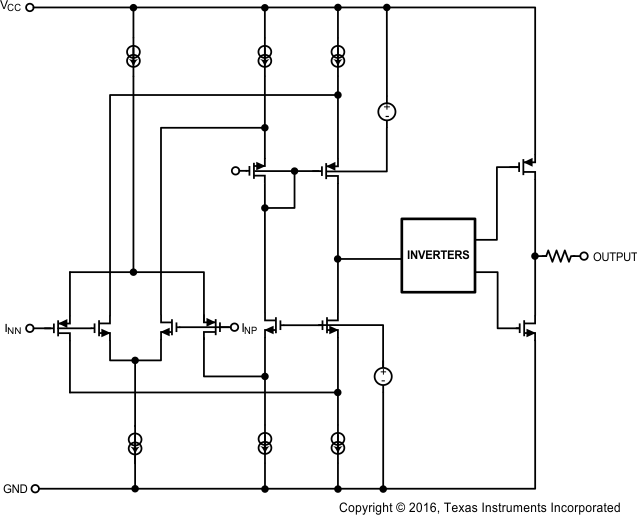
7.3 Feature Description
Low supply current and fast propagation delay distinguish the LPV7215 from other low-power comparators.
7.3.1 Input Stage
The LPV7215 has rail-to-rail input common-mode voltage range. It can operate at any differential input voltage within this limit as long as the differential voltage is greater than zero. A differential input of zero volts may result in oscillation.
The differential input stage of the comparator is a pair of PMOS and NMOS transistors, therefore, no current flows into the device. The input bias current measured is the leakage current in the MOS transistors and input protection diodes. This low bias current allows the comparator to interface with a variety of circuitry and devices with minimal concern about matching the input resistances.
The input to the comparator is protected from excessive voltage by internal ESD diodes connected to both supply rails. This protects the circuit from both ESD events, as well as signals that significantly exceed the supply voltages. When this occurs the ESD protection diodes becomes forward-biased and draws current into these structures, resulting in no input current to the terminals of the comparator. Until this occurs, there is essentially no input current to the diodes. As a result, placing a large resistor in series with an input that may be exposed to large voltages, limits the input current but have no other noticeable effect.
7.3.2 Output Stage
The LPV7215 has a MOS push-pull rail-to-rail output stage. The push-pull transistor configuration of the output keeps the total system power consumption to a minimum. The only current consumed by the LPV7215 is the less than 1-µA supply current and the current going directly into the load. No power is wasted through the pullup resistor when the output is low. The output stage is specifically designed with dead time between the time when one transistor is turned off and the other is turned on (break-before-make) to minimize shoot through currents. The internal logic controls the break-before-make timing of the output transistors. The break-before-make delay varies with temperature and power condition.
7.3.3 Output Current
Even though the LPV7215 uses less than 1-µA supply current, the outputs are able to drive very large currents. The LPV7215 can source up to 17 mA and can sink up to 19 mA, when operated at 5-V supply. This large current handling capability allows driving heavy loads directly.
7.3.4 Response Time
Depending upon the amount of overdrive, the propagation delay is typically 6 to 30 µs. The curves showing propagation delay vs overdrive in the Typical Characteristics section shows the delay time when the input is preset with 100 mV across the inputs and then is driven the other way by 10 mV to 500 mV.
The output signal can show a step during switching depending on the load. A fast RC time constant due to both small capacitive and resistive loads shows a significant step in the output signal. A slow RC time constant due to either a large resistive or capacitive load has a clipped corner on the output signal. The step is observed more prominently during a falling transition from high to low.
The plot in Figure 29 shows the output for single 5-V supply with a 100-kΩ resistor. The step is at 1.3 V.
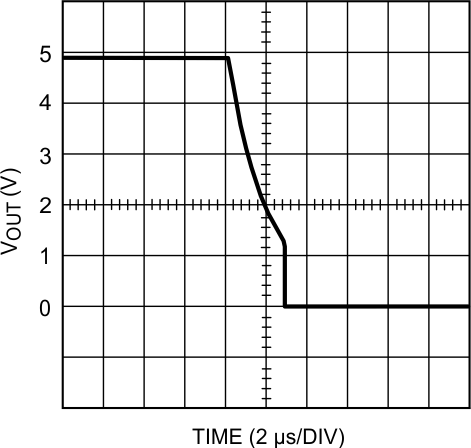 Figure 29. Output Signal Without Capacitive Load
The plot in Figure 30 shows the output signal when a 20-pF capacitor is added as a load. The step is at about 2.5 V.
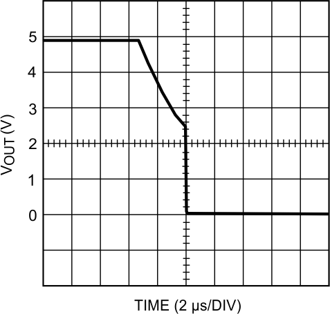 Figure 30. Output Signal With 20-pF Load
7.4 Device Functional Modes
7.4.1 Capacitive and Resistive Loads
The propagation delay is not affected by capacitive loads at the output of the LPV7215. However, resistive loads slightly affect the propagation delay on the falling edge by a reduction of almost 2 µs depending on the load resistance value.
7.4.2 Noise
Most comparators have rather low gain. This allows the output to spend time between high and low when the input signal changes slowly. The result is that the output may oscillate between high and low when the differential input is near zero. The exceptionally high gain of this comparator, 120 dB, eliminates this problem. Less than 1 µV of change on the input drives the output from one rail to the other rail. If the input signal is noisy, the output cannot ignore the noise unless some hysteresis is provided by positive feedback (see Hysteresis).
7.4.3 Hysteresis
To improve propagation delay when low overdrive is needed, hysteresis can be added.
7.4.4 Inverting Comparator With Hysteresis
The inverting comparator with hysteresis requires a three resistor network that is referenced to the supply voltage V+ of the comparator as shown in Figure 31. When VIN at the inverting input is less than VA, the voltage at the noninverting node of the comparator (VIN < VA), the output voltage is high (for simplicity assume VO switches as high as V+). The three network resistors can be represented as R1//R3 in series with R2.
The lower input trip voltage VA1 is defined as Equation 1.
When VIN is greater than VA, the output voltage is low or very close to ground. In this case the three network resistors can be presented as R2//R3 in series with R1.
The upper trip voltage VA2 is defined as Equation 2.
The total hysteresis provided by the network is defined as ΔVA = VA1 – VA2, as shown in Equation 3.

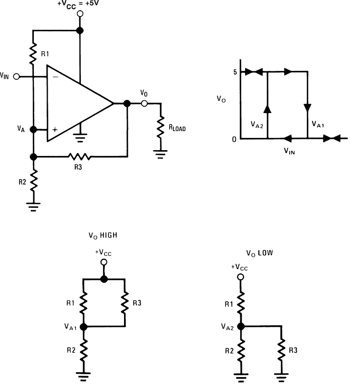 Figure 31. Inverting Comparator With Hysteresis
7.4.5 Noninverting Comparator With Hysteresis
A noninverting comparator with hysteresis requires a two resistor network, and a voltage reference (VREF) at the inverting input. When VIN is low, the output is also low. For the output to switch from low to high, VIN must rise up to VIN1 where VIN1 is calculated by Equation 4.

As soon as VO switches to VCC, VA steps to a value greater than VREF, which is given by Equation 5.

To make the comparator switch back to its low state, VIN must equal VREF before VA again equals VREF. VIN2 can be calculated by Equation 6.

The hysteresis of this circuit is the difference between VIN1 and VIN2, as shown in Equation 7.
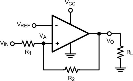 Figure 32. Noninverting Comparator With Hysteresis
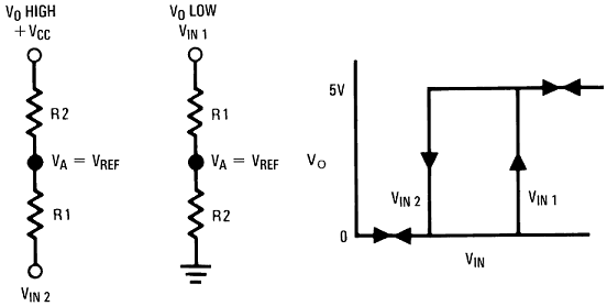 Figure 33. Noninverting Comparator With Hysteresis
7.4.6 Zero Crossing Detector
In a zero crossing detector circuit, the inverting input is connected to ground and the noninverting input is connected to a 100-mVPP AC signal. As the signal at the noninverting input crosses 0 V, the comparator’s output changes state.
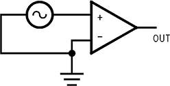 Figure 34. Zero Crossing Detector
To improve switching times and to center the input threshold to ground a small amount of positive feedback is added to the circuit. The voltage divider, R4 and R5, establishes a reference voltage, V1, at the positive input. By making the series resistance, R1 plus R2 equal to R5, the switching condition, V1 = V2, is satisfied when VIN = 0. The positive feedback resistor, R6, is made very large with respect to R5 (R6 = 2000 R5). The resultant hysteresis established by this network is very small (ΔV1 < 10 mV) but it is sufficient to insure rapid output voltage transitions. Diode D1 is used to insure that the inverting input terminal of the comparator never goes below approximately −100 mV. As the input terminal goes negative, D1 will forward bias, clamping the node between R1 and R2 to approximately −700 mV. This sets up a voltage divider with R2 and R3 preventing V2 from going below ground. The maximum negative input overdrive is limited by the current handling ability of D1.
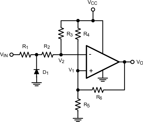 Figure 35. Zero Crossing Detector With Positive Feedback
7.4.7 Threshold Detector
Instead of tying the inverting input to 0 V, the inverting input can be tied to a reference voltage. As the input on the noninverting input passes the VREF threshold, the comparator’s output changes state. It is important to use a stable reference voltage to ensure a consistent switching point.
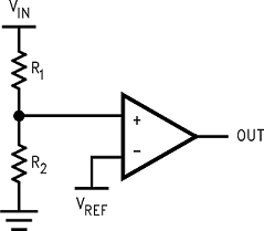 Figure 36. Threshold Detector