JAJSA95J September 2005 – August 2016 LPV7215
PRODUCTION DATA.
- 1 特長
- 2 アプリケーション
- 3 概要
- 4 改訂履歴
- 5 Pin Configuration and Functions
- 6 Specifications
- 7 Detailed Description
- 8 Application and Implementation
- 9 Power Supply Recommendations
- 10Layout
- 11デバイスおよびドキュメントのサポート
- 12メカニカル、パッケージ、および注文情報
パッケージ・オプション
メカニカル・データ(パッケージ|ピン)
サーマルパッド・メカニカル・データ
発注情報
8 Application and Implementation
NOTE
Information in the following applications sections is not part of the TI component specification, and TI does not warrant its accuracy or completeness. TI’s customers are responsible for determining suitability of components for their purposes. Customers should validate and test their design implementation to confirm system functionality.
8.1 Application Information
The LPV7215 is an ultra-low-power comparator with a typical power supply current of 580 nA. It has the best-in-class power supply current versus propagation delay performance available among TI's low-power comparators. The propagation delay is as low as 4.5 µs with 100-mV overdrive at 1.8-V supply.
8.2 Typical Applications
8.2.1 Square Wave Generator
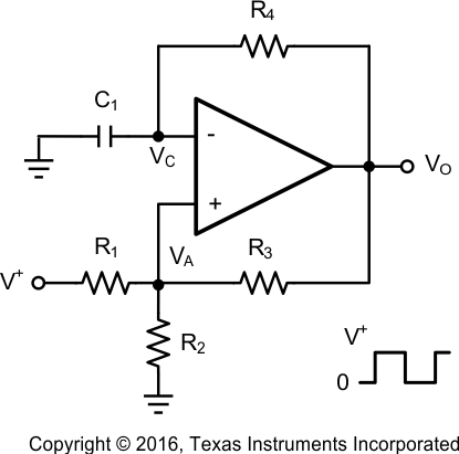 Figure 37. Square Wave Generator Schematic
8.2.1.1 Design Requirements
A typical application for a comparator is as a square wave oscillator. The circuit in Figure 38 generates a square wave whose period is set by the RC time constant of the capacitor C1 and resistor R4. The maximum frequency is limited by the large signal propagation delay of the comparator and by the capacitive loading at the output, which limits the output slew rate.
8.2.1.2 Detailed Design Procedure
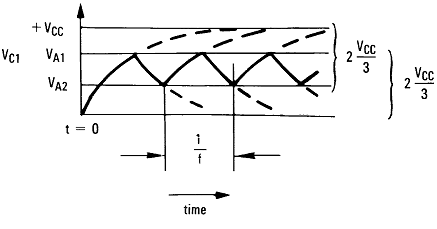 Figure 38. Square Wave Oscillator
Consider the output of Figure 38 to be high to analyze the circuit. That implies that the inverted input (VC) is lower than the noninverting input (VA). This causes the C1 to be charged through R4, and the voltage VC increases until it is equal to the noninverting input. The value of VA at this point is in Equation 8.

If R1 = R2 = R3 then VA1 = 2 VCC/3
At this point the comparator switches pulling down the output to the negative rail. The value of VA at this point, as shown in Equation 9:

If R1 = R2 = R3 then VA2 = VCC/3
The capacitor C1 now discharges through R4, and the voltage VC decreases until it is equal to VA2, at which point the comparator switches again, bringing it back to the initial stage. The time period is equal to twice the time it takes to discharge C1 from 2 VCC/3 to VCC/3, which is given by R4C1 × ln2. Hence the formula for the frequency is given by Equation 10:
8.2.1.3 Application Curves
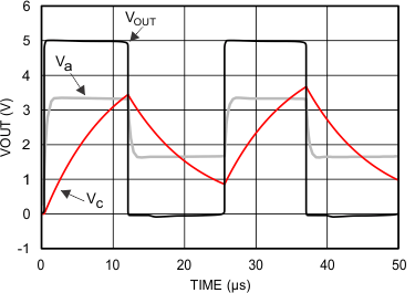
Figure 39 shows the simulated results of an oscillator using the following values:
- R1 = R2 = R3 = R4 = 100 kΩ
- C1 = 100 pF, CL = 20 pF
- V+ = 5 V, V– = GND
- CSTRAY (not shown) from Va to GND = 10 pF
8.2.2 Window Detector
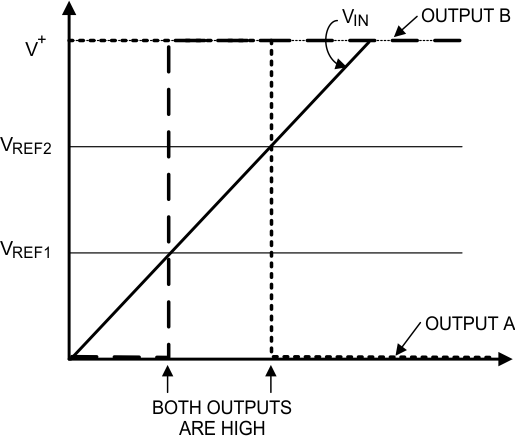
A window detector monitors the input signal to determine if it falls between two voltage levels.
The comparator outputs A and B are high only when VREF1 < VIN < VREF2 or within the window. These are defined as:
Others names for window detectors are: threshold detector, level detectors, and amplitude trigger or detector.
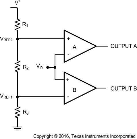 Figure 40. Window Detector
8.2.3 Crystal Oscillator
A simple crystal oscillator using the LPV7215 is shown in Figure 42. Resistors R1 and R2 set the bias point at the comparator’s noninverting input. Resistors, R3 and R4 and capacitor C1 set the inverting input node at an appropriate DC average level based on the output. The crystal’s path provides resonant positive feedback and stable oscillation occurs. The output duty cycle for this circuit is roughly 50%, but it is affected by resistor tolerances and to a lesser extent by the comparator offset.
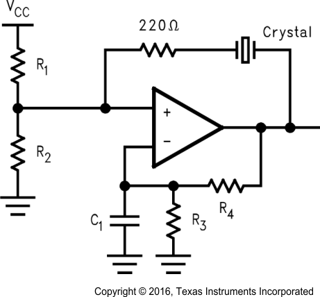 Figure 42. Crystal Oscillator
8.2.4 IR Receiver
The LPV7215 can also be used as an infrared receiver. The infrared photo diode creates a current relative to the amount of infrared light present. The current creates a voltage across RD. When this voltage level crosses the voltage applied by the voltage divider to the inverting input, the output transitions.
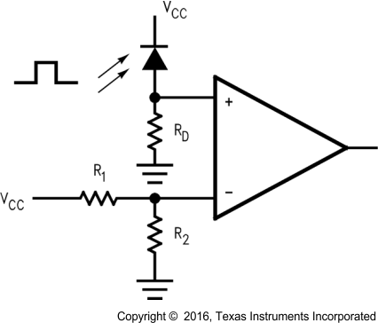 Figure 43. IR Receiver
