JAJSCE6B August 2016 – November 2016 LPV801 , LPV802
PRODUCTION DATA.
10 Layout
10.1 Layout Guidelines
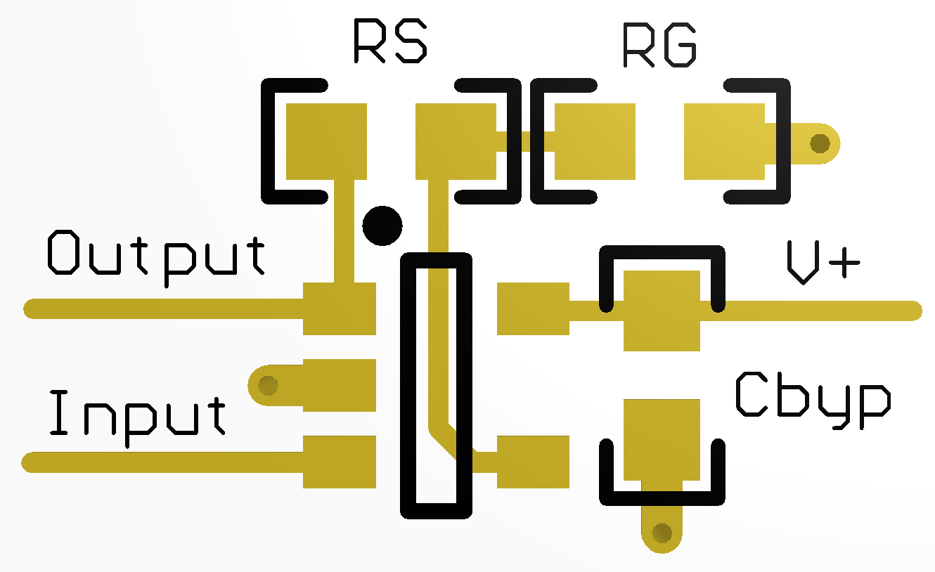
The V+ pin should be bypassed to ground with a low ESR capacitor.
The optimum placement is closest to the V+ and ground pins.
Care should be taken to minimize the loop area formed by the bypass capacitor connection between V+ and ground.
The ground pin should be connected to the PCB ground plane at the pin of the device.
The feedback components should be placed as close to the device as possible to minimize strays.
10.2 Layout Example
 Figure 42. SOT-23 Layout Example (Top View)