JAJSQL9C may 2018 – august 2023 LV3842
ADVANCE INFORMATION
- 1
- 1 特長
- 2 アプリケーション
- 3 概要
- 4 Revision History
- 5 Device Comparison Table
- 6 Pin Configuration and Functions
- 7 Specifications
- 8 Detailed Description
- 9 Application and Implementation
- 10Device and Documentation Support
- 11Mechanical, Packaging, and Orderable Information
9.2.2.3 Output Capacitor Selection
The device is designed to be used with a wide variety of LC filters. It is generally desired to use as little output capacitance as possible to keep cost and size down. The output capacitors, COUT, must be chosen with care because it directly affects the steady state output voltage ripple, loop stability and the voltage over/undershoot during load current transients. The output voltage ripple is essentially composed of two parts. One is caused by the inductor current ripple going through the Equivalent Series Resistance (ESR) of the output capacitors:

The other is caused by the inductor current ripple charging and discharging the output capacitors:
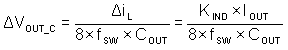
The two components in the voltage ripple are not in phase, so the actual peak-to-peak ripple is smaller than the sum of the two peaks.
Output capacitance is usually limited by transient performance specifications if the system requires tight voltage regulation with presence of large current steps and fast slew rate. When a large load step happens, output capacitors provide the required charge before the inductor current can slew up to the appropriate level. The regulator control loop usually needs 8 or more clock cycles to regulate the inductor current equal to the new load level. The output capacitance must be large enough to supply the current difference for 8 clock cycles to maintain the output voltage within the specified range. Equation 12 shows the minimum output capacitance needed for specified output over/undershoot.
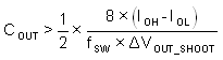
where
- KIND = Ripple ratio of the inductor ripple current (ΔiL / IOUT)
- IOL = Low level output current during load transient
- IOH = High level output current during load transient
- VOUT_SHOOT = Target output voltage over/undershoot
For this design example, the target output ripple is 30 mV. Presuppose ΔVOUT_ESR = ΔVOUT_C = 30 mV, and chose KIND = 0.4. Equation 10 yields ESR no larger than 125 mΩ and Equation 11 yields COUT no smaller than 0.91 µF. For the target over/undershoot range of this design, ΔVOUT_SHOOT = 5% × VOUT = 250 mV. The COUT can be calculated to be no smaller than 8.3 µF by Equation 12. In summary, the most stringent criteria for the output capacitor is 8.3 µF. Consider of derating, one 22 µF, 10 V, X7R ceramic capacitor with 10 mΩ ESR is used.