JAJSQL9C may   2018  – august 2023 LV3842

ADVANCE INFORMATION  

  1.   1
  2. 特長
  3. アプリケーション
  4. 概要
  5. Revision History
  6. Device Comparison Table
  7. Pin Configuration and Functions
  8. Specifications
    1. 7.1 Absolute Maximum Ratings
    2. 7.2 ESD Ratings
    3. 7.3 Recommended Operating Conditions
    4. 7.4 Thermal Information
    5. 7.5 Electrical Characteristics
    6. 7.6 Timing Requirements
    7. 7.7 Switching Characteristics
    8. 7.8 Typical Characteristics
  9. Detailed Description
    1. 8.1 Overview
    2. 8.2 Functional Block Diagram
    3. 8.3 Feature Description
      1. 8.3.1 Fixed Frequency Peak Current Mode Control
      2. 8.3.2 Adjustable Output Voltage
      3. 8.3.3 Enable
      4. 8.3.4 Minimum ON-Time, Minimum OFF-Time and Frequency Foldback
      5. 8.3.5 Bootstrap Voltage
      6. 8.3.6 Overcurrent and Short-Circuit Protection
      7. 8.3.7 Soft Start
      8. 8.3.8 Thermal Shutdown
    4. 8.4 Device Functional Modes
      1. 8.4.1 Shutdown Mode
      2. 8.4.2 Active Mode
      3. 8.4.3 CCM Mode
      4. 8.4.4 Light-Load Operation (PFM Version)
      5. 8.4.5 Light-Load Operation (FPWM Version)
  10. Application and Implementation
    1. 9.1 Application Information
    2. 9.2 Typical Application
      1. 9.2.1 Design Requirements
      2. 9.2.2 Detailed Design Procedure
        1. 9.2.2.1 Output Voltage Set-Point
        2. 9.2.2.2 Inductor Selection
        3. 9.2.2.3 Output Capacitor Selection
        4. 9.2.2.4 Input Capacitor Selection
        5. 9.2.2.5 Bootstrap Capacitor
        6. 9.2.2.6 Undervoltage Lockout Set-Point
      3. 9.2.3 Application Curves
    3. 9.3 Power Supply Recommendations
    4. 9.4 Layout
      1. 9.4.1 Layout Guidelines
      2. 9.4.2 Compact Layout for EMI Reduction
      3. 9.4.3 Feedback Resistors
      4. 9.4.4 Layout Example
  11. 10Device and Documentation Support
    1. 10.1 Documentation Support
      1. 10.1.1 Related Documentation
    2. 10.2 ドキュメントの更新通知を受け取る方法
    3. 10.3 サポート・リソース
    4. 10.4 Trademarks
    5. 10.5 静電気放電に関する注意事項
    6. 10.6 用語集
  12. 11Mechanical, Packaging, and Orderable Information
    1. 11.1 Tape and Reel Information

パッケージ・オプション

メカニカル・データ(パッケージ|ピン)
サーマルパッド・メカニカル・データ
発注情報

Minimum ON-Time, Minimum OFF-Time and Frequency Foldback

Minimum ON-time, TON_MIN, is the smallest duration of time that the HS switch can be on. TON_MIN is typically 70 ns in the LV3842 . Minimum OFF-time, TOFF_MIN, is the smallest duration that the HS switch can be off. TOFF_MIN is typically 100 ns. In CCM operation, TON_MIN and TOFF_MIN limit the voltage conversion ratio without switching frequency foldback.

The minimum duty cycle without frequency foldback allowed is

Equation 2. DMIN = TON_MIN X fSW

The maximum duty cycle without frequency foldback allowed is

Equation 3. DMAX = 1 - TOFF_MIN X fSW

Given a required output voltage, the maximum VIN without frequency foldback can be found by

Equation 4. GUID-34F33FC3-C60A-4A09-AF4A-8D4A2B095AA5-low.gif

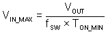
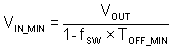
The minimum VIN without frequency foldback can be calculated by

Equation 5. GUID-D902D2CC-3C49-4A06-ACC5-DE0B7390B60C-low.gif

In the LV3842, a frequency foldback scheme is employed after the TON_MIN or TOFF_MIN is triggered, which can extend the maximum duty cycle or lower the minimum duty cycle.

The on-time decreases while VIN voltage increases. After the on-time decreases to TON_MIN, the switching frequency starts to decrease while VIN continues to go up, which lowers the duty cycle further to keep VOUT in regulation according to Equation 2.

The frequency foldback scheme also works after larger duty cycle is needed under low VIN conditions. The frequency decreases after the device hits its TOFF_MIN, which extends the maximum duty cycle according to Equation 3. In such condition, the frequency can be as low as about 133-kHz minimum. Wide range of frequency foldback allows the LV3842 output voltage stay in regulation with a much lower supply voltage VIN. This leads to a lower effective drop-out voltage.

With frequency foldback, VIN_MAX is raised, and VIN_MIN is lowered to overcome TON_MIN or TOFF_MIN limitation.

GUID-12115C0A-48D3-4F15-943F-A7F08025BE64-low.png
VOUT = 1 V
Figure 8-4 Frequency Foldback at TON_MIN
GUID-D66DD095-4FF7-4736-B6BE-BE33C23B9F04-low.png
VOUT = 5 V
Figure 8-5 Frequency Foldback at TOFF_MIN