JAJSQL9C may 2018 – august 2023 LV3842
ADVANCE INFORMATION
- 1
- 1 特長
- 2 アプリケーション
- 3 概要
- 4 Revision History
- 5 Device Comparison Table
- 6 Pin Configuration and Functions
- 7 Specifications
- 8 Detailed Description
- 9 Application and Implementation
- 10Device and Documentation Support
- 11Mechanical, Packaging, and Orderable Information
8.3.6 Overcurrent and Short-Circuit Protection
The LV3842 is protected from overcurrent conditions by cycle-by-cycle current limit on both the peak and valley of the inductor current. Hiccup mode is activated if a fault condition persists to prevent over-heating.
High-side MOSFET overcurrent protection is implemented by the nature of the Peak Current Mode control. The HS switch current is sensed when the HS is turned on after a set blanking time. The HS switch current is compared to the output of the Error Amplifier (EA) minus slope compensation every switching cycle. Please refer to Section 8.2 for more details. The peak current of HS switch is limited by a clamped maximum peak current threshold IHS_LIMIT which is constant.
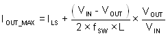
The current going through LS MOSFET is also sensed and monitored. When the LS switch turns on, the inductor current begins to ramp down. The LS switch is not turned OFF at the end of a switching cycle if its current is above the LS current limit ILS_LIMIT. The LS switch is kept ON so that inductor current keeps ramping down, until the inductor current ramps below the LS current limit ILS_LIMIT. Then the LS switch is turned OFF and the HS switch is turned on after a dead time. This is somewhat different to the more typical peak current limit, and results in Equation 6 for the maximum load current.
If the feedback voltage is lower than 40% of the VREF, the current of the LS switch triggers LS current limit for 256 consecutive cycles, hiccup current protection mode is activated. In hiccup mode, the regulator shuts down and keeps off for a period of hiccup, THICCUP (135-ms typical), before the LV3842 tries to start again. If overcurrent or short-circuit fault condition still exist, hiccup repeats until the fault condition is removed. Hiccup mode reduces power dissipation under severe over-current conditions, prevents over-heating and potential damage to the device.
For FPWM version, the inductor current is allowed to go negative. If this current exceeds the LS negative current limit ILS_NEG, the LS switch is turned off and HS switch is turned on immediately. This is used to protect the LS switch from excessive negative current.