JAJSQL9C may 2018 – august 2023 LV3842
ADVANCE INFORMATION
- 1
- 1 特長
- 2 アプリケーション
- 3 概要
- 4 Revision History
- 5 Device Comparison Table
- 6 Pin Configuration and Functions
- 7 Specifications
- 8 Detailed Description
- 9 Application and Implementation
- 10Device and Documentation Support
- 11Mechanical, Packaging, and Orderable Information
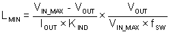
9.2.2.2 Inductor Selection
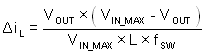
The most critical parameters for the inductor are the inductance, saturation current and the RMS current. The inductance is based on the desired peak-to-peak ripple current ΔiL. Because the ripple current increases with the input voltage, the maximum input voltage is always used to calculate the minimum inductance LMIN. Use Equation 9 to calculate the minimum value of the output inductor. KIND is a coefficient that represents the amount of inductor ripple current relative to the maximum output current of the device. A reasonable value of KIND must be 20% – 40%. During an instantaneous over current operation event, the RMS and peak inductor current can be high. The inductor current rating must be a bit higher than current limit.
In general, it is preferable to choose lower inductance in switching power supplies, because it usually corresponds to faster transient response, smaller DCR, and reduced size for more compact designs. But too low of an inductance can generate too large of an inductor current ripple such that over current protection at the full load can be falsely triggered. It also generates more inductor core loss because the current ripple is larger. Larger inductor current ripple also implies larger output voltage ripple with same output capacitors. With peak current mode control, TI does note recommend to have too small of an inductor current ripple. A larger peak current ripple improves the comparator signal to noise ratio.
For this design example, choose KIND = 0.4, the minimum inductor value is calculated to be 16.3 µH. Choose the nearest standard 18 µH ferrite inductor with a capability of 1 A RMS current and 1.5 A saturation current.