JAJSTR9D May 1980 – March 2024 MC3487
PRODUCTION DATA
- 1
- 1 特長
- 2 アプリケーション
- 3 概要
- 4 Pin Configuration and Functions
- 5 Specifications
- 6 Parameter Measurement Information
- 7 Device Functional Modes
- 8 Device and Documentation Support
- 9 Revision History
- 10Mechanical, Packaging, and Orderable Information
パッケージ・オプション
デバイスごとのパッケージ図は、PDF版データシートをご参照ください。
メカニカル・データ(パッケージ|ピン)
- NS|16
- N|16
- D|16
サーマルパッド・メカニカル・データ
発注情報
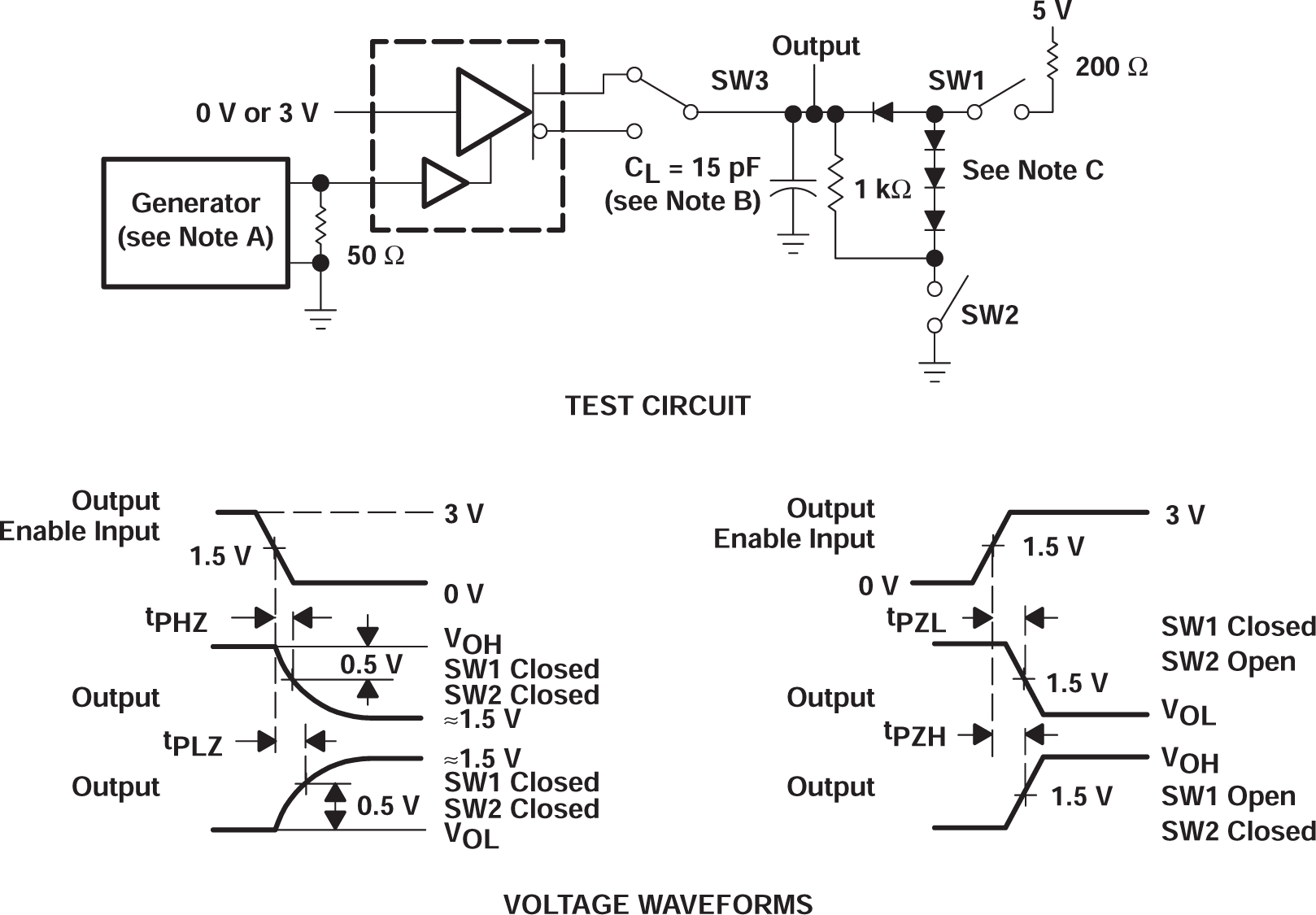
6 Parameter Measurement Information
 Figure 6-1 Differential and Common-Mode Output Voltages
A. The input pulse is supplied by a generator having the following characteristics: tr ≤ 5 ns, tf ≤ 5 ns, PRR ≤ 1 MHz, duty cycle = 50% ZO = 50 Ω.
B. CL includes probe and stray capacitance.
C. All diodes are 1N916 or 1N3064.
Figure 6-2 Test Circuit and Voltage Waveforms
A. The input pulse is supplied by a generator having the following characteristics: tr ≤ 5 ns, tf ≤ 5 ns, PRR ≤ 1 MHz, duty cycle = 50%, ZO = 50 Ω.
B. CL includes probe and stray capacitance.
Figure 6-3 Test Circuit and Voltage Waveforms
A. The input pulse is supplied by a generator having the following characteristics: tr ≤ 5 ns, tf ≤ 5 ns, PRR ≤ 1 MHz, duty cycle = 50%, ZO = 50 Ω.
B. CL includes probe and stray capacitance.
C. All diodes are 1N916 or 1N3064.
Figure 6-4 Driver Test Circuit and Voltage Waveforms