JAJSNT0A december   2022  – april 2023 MCT8315A

PRODUCTION DATA  

  1.   1
  2. 特長
  3. アプリケーション
  4. 概要
  5. Revision History
  6. Pin Configuration and Functions
  7. Specifications
    1. 6.1 Absolute Maximum Ratings
    2. 6.2 ESD Ratings
    3. 6.3 Recommended Operating Conditions
    4. 6.4 Thermal Information
    5. 6.5 Electrical Characteristics
    6. 6.6 Characteristics of the SDA and SCL bus for Standard and Fast mode
    7. 6.7 Typical Characteristics
  8. Detailed Description
    1. 7.1 Overview
    2. 7.2 Functional Block Diagram
    3. 7.3 Feature Description
      1. 7.3.1  Output Stage
      2. 7.3.2  Device Interface
        1. 7.3.2.1 Interface - Control and Monitoring
        2. 7.3.2.2 I2C Interface
      3. 7.3.3  Step-Down Mixed-Mode Buck Regulator
        1. 7.3.3.1 Buck in Inductor Mode
        2. 7.3.3.2 Buck in Resistor mode
        3. 7.3.3.3 Buck Regulator with External LDO
        4. 7.3.3.4 AVDD Power Sequencing from Buck Regulator
        5. 7.3.3.5 Mixed Mode Buck Operation and Control
        6. 7.3.3.6 Buck Under Voltage Protection
        7. 7.3.3.7 Buck Over Current Protection
      4. 7.3.4  AVDD Linear Voltage Regulator
      5. 7.3.5  Charge Pump
      6. 7.3.6  Slew Rate Control
      7. 7.3.7  Cross Conduction (Dead Time)
      8. 7.3.8  Speed Control
        1. 7.3.8.1 Analog Mode Speed Control
        2. 7.3.8.2 PWM Mode Speed Control
        3. 7.3.8.3 I2C based Speed Control
        4. 7.3.8.4 Frequency Mode Speed Control
      9. 7.3.9  Starting the Motor Under Different Initial Conditions
        1. 7.3.9.1 Case 1 – Motor is Stationary
        2. 7.3.9.2 Case 2 – Motor is Spinning in the Forward Direction
        3. 7.3.9.3 Case 3 – Motor is Spinning in the Reverse Direction
      10. 7.3.10 Motor Start Sequence (MSS)
        1. 7.3.10.1 Initial Speed Detect (ISD)
        2. 7.3.10.2 Motor Resynchronization
        3. 7.3.10.3 Reverse Drive
        4. 7.3.10.4 Motor Start-up
          1. 7.3.10.4.1 Align
          2. 7.3.10.4.2 Double Align
          3. 7.3.10.4.3 Initial Position Detection (IPD)
            1. 7.3.10.4.3.1 IPD Operation
            2. 7.3.10.4.3.2 IPD Release Mode
            3. 7.3.10.4.3.3 IPD Advance Angle
          4. 7.3.10.4.4 Slow First Cycle Startup
          5. 7.3.10.4.5 Open loop
          6. 7.3.10.4.6 Transition from Open to Closed Loop
      11. 7.3.11 Closed Loop Operation
        1. 7.3.11.1 120o Commutation
          1. 7.3.11.1.1 High-Side Modulation
          2. 7.3.11.1.2 Low-Side Modulation
          3. 7.3.11.1.3 Mixed Modulation
        2. 7.3.11.2 Variable Commutation
        3. 7.3.11.3 Lead Angle Control
        4. 7.3.11.4 Closed loop accelerate
      12. 7.3.12 Speed Loop
      13. 7.3.13 Input Power Regulation
      14. 7.3.14 Anti-Voltage Surge (AVS)
      15. 7.3.15 Output PWM Switching Frequency
      16. 7.3.16 Fast Start-up (< 50 ms)
        1. 7.3.16.1 BEMF Threshold
        2. 7.3.16.2 Dynamic Degauss
      17. 7.3.17 Fast Deceleration
      18. 7.3.18 Active Demagnetization
        1. 7.3.18.1 Active Demagnetization in action
      19. 7.3.19 Motor Stop Options
        1. 7.3.19.1 Coast (Hi-Z) Mode
        2. 7.3.19.2 Recirculation Mode
        3. 7.3.19.3 Low-Side Braking
        4. 7.3.19.4 High-Side Braking
        5. 7.3.19.5 Active Spin-Down
      20. 7.3.20 FG Configuration
        1. 7.3.20.1 FG Output Frequency
        2. 7.3.20.2 FG Open-Loop and Lock Behavior
      21. 7.3.21 Protections
        1. 7.3.21.1  VM Supply Undervoltage Lockout
        2. 7.3.21.2  AVDD Undervoltage Lockout (AVDD_UV)
        3. 7.3.21.3  BUCK Undervoltage Lockout (BUCK_UV)
        4. 7.3.21.4  VCP Charge Pump Undervoltage Lockout (CPUV)
        5. 7.3.21.5  Overvoltage Protection (OVP)
        6. 7.3.21.6  Overcurrent Protection (OCP)
          1. 7.3.21.6.1 OCP Latched Shutdown (OCP_MODE = 00b)
          2. 7.3.21.6.2 OCP Automatic Retry (OCP_MODE = 01b)
          3. 7.3.21.6.3 OCP Report Only (OCP_MODE = 10b)
          4. 7.3.21.6.4 OCP Disabled (OCP_MODE = 11b)
        7. 7.3.21.7  Buck Overcurrent Protection
        8. 7.3.21.8  Cycle-by-Cycle (CBC) Current Limit (CBC_ILIMIT)
          1. 7.3.21.8.1 CBC_ILIMIT Automatic Recovery next PWM Cycle (CBC_ILIMIT_MODE = 000xb)
          2. 7.3.21.8.2 CBC_ILIMIT Automatic Recovery Threshold Based (CBC_ILIMIT_MODE = 001xb)
          3. 7.3.21.8.3 CBC_ILIMIT Automatic Recovery after 'n' PWM Cycles (CBC_ILIMIT_MODE = 010xb)
          4. 7.3.21.8.4 CBC_ILIMIT Report Only (CBC_ILIMIT_MODE = 0110b)
          5. 7.3.21.8.5 CBC_ILIMIT Disabled (CBC_ILIMIT_MODE = 0111b or 1xxxb)
        9. 7.3.21.9  Lock Detection Current Limit (LOCK_ILIMIT)
          1. 7.3.21.9.1 LOCK_ILIMIT Latched Shutdown (LOCK_ILIMIT_MODE = 00xxb)
          2. 7.3.21.9.2 LOCK_ILIMIT Automatic Recovery (LOCK_ILIMIT_MODE = 01xxb)
          3. 7.3.21.9.3 LOCK_ILIMIT Report Only (LOCK_ILIMIT_MODE = 1000b)
          4. 7.3.21.9.4 LOCK_ILIMIT Disabled (LOCK_ILIMIT_MODE = 1xx1b)
        10. 7.3.21.10 Thermal Warning (OTW)
        11. 7.3.21.11 Thermal Shutdown (TSD)
        12. 7.3.21.12 Motor Lock (MTR_LCK)
          1. 7.3.21.12.1 MTR_LCK Latched Shutdown (MTR_LCK_MODE = 00xxb)
          2. 7.3.21.12.2 MTR_LCK Automatic Recovery (MTR_LCK_MODE= 01xxb)
          3. 7.3.21.12.3 MTR_LCK Report Only (MTR_LCK_MODE = 1000b)
          4. 7.3.21.12.4 MTR_LCK Disabled (MTR_LCK_MODE = 1xx1b)
        13. 7.3.21.13 Motor Lock Detection
          1. 7.3.21.13.1 Lock 1: Abnormal Speed (ABN_SPEED)
          2. 7.3.21.13.2 Lock 2: Loss of Sync (LOSS_OF_SYNC)
          3. 7.3.21.13.3 Lock3: No-Motor Fault (NO_MTR)
        14. 7.3.21.14 SW VM Undervoltage Protection
        15. 7.3.21.15 SW VM Overvoltage Protection
        16. 7.3.21.16 IPD Faults
    4. 7.4 Device Functional Modes
      1. 7.4.1 Functional Modes
        1. 7.4.1.1 Sleep Mode
        2. 7.4.1.2 Standby Mode
        3. 7.4.1.3 Fault Reset (CLR_FLT)
    5. 7.5 External Interface
      1. 7.5.1 DRVOFF Functionality
      2. 7.5.2 DAC outputs
      3. 7.5.3 Current Sense Output
      4. 7.5.4 Oscillator Source
        1. 7.5.4.1 External Clock Source
      5. 7.5.5 External Watchdog
    6. 7.6 EEPROM access and I2C interface
      1. 7.6.1 EEPROM Access
        1. 7.6.1.1 EEPROM Write
        2. 7.6.1.2 EEPROM Read
      2. 7.6.2 I2C Serial Interface
        1. 7.6.2.1 I2C Data Word
        2. 7.6.2.2 I2C Write Transaction
        3. 7.6.2.3 I2C Read Transaction
        4. 7.6.2.4 I2C Communication Protocol Packet Examples
        5. 7.6.2.5 I2C Clock Stretching
        6. 7.6.2.6 CRC Byte Calculation
    7. 7.7 EEPROM (Non-Volatile) Register Map
      1. 7.7.1 Algorithm_Configuration Registers
      2. 7.7.2 Fault_Configuration Registers
      3. 7.7.3 Hardware_Configuration Registers
      4. 7.7.4 Gate_Driver_Configuration Registers
    8. 7.8 RAM (Volatile) Register Map
      1. 7.8.1 Fault_Status Registers
      2. 7.8.2 System_Status Registers
      3. 7.8.3 Algo_Control Registers
      4. 7.8.4 Device_Control Registers
      5. 7.8.5 Algorithm_Variables Registers
  9. Application and Implementation
    1. 8.1 Application Information
    2. 8.2 Typical Applications
      1. 8.2.1 Application curves
        1. 8.2.1.1 Motor startup
        2. 8.2.1.2 120o and variable commutation
        3. 8.2.1.3 Faster startup time
        4. 8.2.1.4 Setting the BEMF threshold
        5. 8.2.1.5 Maximum speed
        6. 8.2.1.6 Faster deceleration
  10. Power Supply Recommendations
    1. 9.1 Bulk Capacitance
  11. 10Layout
    1. 10.1 Layout Guidelines
    2. 10.2 Layout Example
    3. 10.3 Thermal Considerations
      1. 10.3.1 Power Dissipation
  12. 11Device and Documentation Support
    1. 11.1 サポート・リソース
    2. 11.2 Trademarks
    3. 11.3 静電気放電に関する注意事項
    4. 11.4 用語集
  13. 12Mechanical, Packaging, and Orderable Information
    1. 12.1 Tape and Reel Information

パッケージ・オプション

メカニカル・データ(パッケージ|ピン)
サーマルパッド・メカニカル・データ
発注情報

Active Demagnetization in action

Figure 7-40 shows the operation of active demagnetization during the BLDC motor commutation. As shown in Figure 7-40 (a), the current is flowing from HA to LC in one commutation state. During the commutation change over as shown in Figure 7-40 (b), the HB FET is turned ON (and HA FET is turned OFF), and the commutation current (due to motor inductance) in OUTA flows through the body diode of LA. This results in a higher diode loss depending on the commutation current. This commutation loss is reduced by turning on the LA FET for the commutation time as shown in Figure 7-40 (c).

Similarly, the active demagnetization operation of a high-side FET is realized in Figure 7-40 (d), (e) and (f).

GUID-A76774AB-4868-4F6B-A832-4CD2B91A8123-low.gifFigure 7-40 Active Demagnetization in BLDC Motor Commutation

Figure 7-41 (a) shows the BLDC motor phase current waveforms with Active Demagnetization with trapezoidal commutation. This figure shows the operation of various switches in a single commutation cycle.

Figure 7-41 (b) shows the zoomed waveform of commutation cycle.
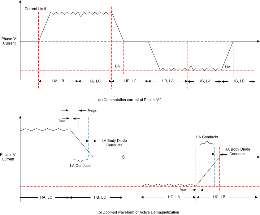
GUID-F98E1938-36A8-4313-ADB4-1084A850E43C-low.gifFigure 7-41 Current Waveforms with Active Demagnetization