JAJSEA9A December 2017 – March 2018 MSP430FR5969-SP
PRODUCTION DATA.
- 1デバイスの概要
- 2改訂履歴
- 3Terminal Configuration and Functions
-
4Specifications
- 4.1 Absolute Maximum Ratings
- 4.2 ESD Ratings
- 4.3 Recommended Operating Conditions
- 4.4 Active Mode Supply Current Into VCC Excluding External Current
- 4.5 Typical Characteristics – Active Mode Supply Currents
- 4.6 Low-Power Mode (LPM0, LPM1) Supply Currents Into VCC Excluding External Current
- 4.7 Low-Power Mode (LPM2, LPM3, LPM4) Supply Currents (Into VCC) Excluding External Current
- 4.8 Low-Power Mode (LPM3.5, LPM4.5) Supply Currents (Into VCC) Excluding External Current
- 4.9 Typical Characteristics, Current Consumption per Module
- 4.10 Thermal Resistance Characteristics
- 4.11
Timing and Switching Characteristics
- 4.11.1 Power Supply Sequencing
- 4.11.2 Reset Timing
- 4.11.3 Clock Specifications
- 4.11.4 Wake-up Characteristics
- 4.11.5 Digital I/Os
- 4.11.6 Timer_A and Timer_B
- 4.11.7 eUSCI
- 4.11.8
ADC
- Table 4-22 12-Bit ADC, Power Supply and Input Range Conditions
- Table 4-23 12-Bit ADC, Timing Parameters
- Table 4-24 12-Bit ADC, Linearity Parameters With External Reference
- Table 4-25 12-Bit ADC, Dynamic Performance for Differential Inputs With External Reference
- Table 4-26 12-Bit ADC, Dynamic Performance for Differential Inputs With Internal Reference
- Table 4-27 12-Bit ADC, Dynamic Performance for Single-Ended Inputs With External Reference
- Table 4-28 12-Bit ADC, Dynamic Performance for Single-Ended Inputs With Internal Reference
- Table 4-29 12-Bit ADC, Dynamic Performance With 32.768-kHz Clock
- Table 4-30 12-Bit ADC, Temperature Sensor and Built-In V1/2
- Table 4-31 12-Bit ADC, External Reference
- 4.11.9 Reference
- 4.11.10 Comparator
- 4.11.11 FRAM
- 4.12 Emulation and Debug
-
5Detailed Description
- 5.1 Overview
- 5.2 CPU
- 5.3 Operating Modes
- 5.4 Interrupt Vector Table and Signatures
- 5.5 Memory Organization
- 5.6 Bootloader (BSL)
- 5.7 JTAG Operation
- 5.8 FRAM
- 5.9 Memory Protection Unit Including IP Encapsulation
- 5.10
Peripherals
- 5.10.1 Digital I/O
- 5.10.2 Oscillator and Clock System (CS)
- 5.10.3 Power-Management Module (PMM)
- 5.10.4 Hardware Multiplier (MPY)
- 5.10.5 Real-Time Clock (RTC_B) (Only MSP430FR596x and MSP430FR594x)
- 5.10.6 Watchdog Timer (WDT_A)
- 5.10.7 System Module (SYS)
- 5.10.8 DMA Controller
- 5.10.9 Enhanced Universal Serial Communication Interface (eUSCI)
- 5.10.10 TA0, TA1
- 5.10.11 TA2, TA3
- 5.10.12 TB0
- 5.10.13 ADC12_B
- 5.10.14 Comparator_E
- 5.10.15 CRC16
- 5.10.16 AES256 Accelerator
- 5.10.17 True Random Seed
- 5.10.18 Shared Reference (REF)
- 5.10.19 Embedded Emulation
- 5.10.20 Peripheral File Map
- 5.11
Input and Output Diagrams
- 5.11.1 Port P1 (P1.0 to P1.2) Input/Output With Schmitt Trigger
- 5.11.2 Port P1 (P1.3 to P1.5) Input/Output With Schmitt Trigger
- 5.11.3 Port P1 (P1.6 and P1.7) Input/Output With Schmitt Trigger
- 5.11.4 Port P2 (P2.0 to P2.2) Input/Output With Schmitt Trigger
- 5.11.5 Port P2 (P2.3 and P2.4) Input/Output With Schmitt Trigger
- 5.11.6 Port P2 (P2.5 and P2.6) Input/Output With Schmitt Trigger
- 5.11.7 Port P2 (P2.7) Input/Output With Schmitt Trigger
- 5.11.8 Port P3 (P3.0 to P3.3) Input/Output With Schmitt Trigger
- 5.11.9 Port P3 (P3.4 to P3.7) Input/Output With Schmitt Trigger
- 5.11.10 Port P4 (P4.0 to P4.3) Input/Output With Schmitt Trigger
- 5.11.11 Port P4 (P4.4 to P4.7) Input/Output With Schmitt Trigger
- 5.11.12 Port PJ, PJ.4 and PJ.5 Input/Output With Schmitt Trigger
- 5.11.13 Port PJ (PJ.6 and PJ.7) Input/Output With Schmitt Trigger
- 5.11.14 Port PJ (PJ.0 to PJ.3) JTAG Pins TDO, TMS, TCK, TDI/TCLK, Input/Output With Schmitt Trigger
- 5.12 Device Descriptor (TLV)
- 5.13 Identification
- 6Applications, Implementation, and Layout
- 7デバイスおよびドキュメントのサポート
- 8メカニカル、パッケージ、および注文情報
パッケージ・オプション
メカニカル・データ(パッケージ|ピン)
サーマルパッド・メカニカル・データ
発注情報
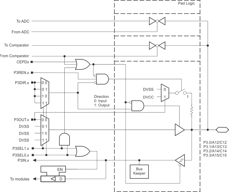
5.11.8 Port P3 (P3.0 to P3.3) Input/Output With Schmitt Trigger
Figure 5-9 shows the port diagram. Table 5-54 summarizes the selection of the pin function.
Table 5-54 Port P3 (P3.0 to P3.3) Pin Functions
| PIN NAME (P3.x) | x | FUNCTION | CONTROL BITS AND SIGNALS(1) | ||
|---|---|---|---|---|---|
| P3DIR.x | P3SEL1.x | P3SEL0.x | |||
| P3.0/A12/C12 | 0 | P3.0 (I/O) | I: 0; O: 1 | 0 | 0 |
| N/A | 0 | 0 | 1 | ||
| Internally tied to DVSS | 1 | ||||
| N/A | 0 | 1 | 0 | ||
| Internally tied to DVSS | 1 | ||||
| A12/C12(1)(2) | X | 1 | 1 | ||
| P3.1/A13/C13 | 1 | P3.1 (I/O) | I: 0; O: 1 | 0 | 0 |
| N/A | 0 | 0 | 1 | ||
| Internally tied to DVSS | 1 | ||||
| N/A | 0 | 1 | 0 | ||
| Internally tied to DVSS | 1 | ||||
| A13/C13(1)(2) | X | 1 | 1 | ||
| P3.2/A14/C14 | 2 | P3.2 (I/O) | I: 0; O: 1 | 0 | 0 |
| N/A | 0 | 0 | 1 | ||
| Internally tied to DVSS | 1 | ||||
| N/A | 0 | 1 | 0 | ||
| Internally tied to DVSS | 1 | ||||
| A14/C14(1)(2) | X | 1 | 1 | ||
| P3.3/A15/C15 | 3 | P3.3 (I/O) | I: 0; O: 1 | 0 | 0 |
| N/A | 0 | 0 | 1 | ||
| Internally tied to DVSS | 1 | ||||
| N/A | 0 | 1 | 0 | ||
| Internally tied to DVSS | 1 | ||||
| A15/C15(1)(2) | X | 1 | 1 | ||
(1) Setting P3SEL1.x and P3SEL0.x disables the output driver and the input Schmitt trigger to prevent parasitic cross currents when applying analog signals.
(2) Setting the CEPDx bit of the comparator disables the output driver and the input Schmitt trigger to prevent parasitic cross currents when applying analog signals. Selecting the Cx input pin to the comparator multiplexer with the input select bits in the comparator module automatically disables output driver and input buffer for that pin, regardless of the state of the associated CEPDx bit.
