JAJSCO7A November 2016 – November 2017 MUX506 , MUX507
PRODUCTION DATA.
- 1 特長
- 2 アプリケーション
- 3 概要
- 4 改訂履歴
- 5 Pin Configuration and Functions
- 6 Specifications
- 7 Parameter Measurement Information
- 8 Detailed Description
- 9 Application and Implementation
- 10Power Supply Recommendations
- 11Layout
- 12デバイスおよびドキュメントのサポート
- 13メカニカル、パッケージ、および注文情報
パッケージ・オプション
メカニカル・データ(パッケージ|ピン)
サーマルパッド・メカニカル・データ
- DW|28
発注情報
9 Application and Implementation
NOTE
Information in the following applications sections is not part of the TI component specification, and TI does not warrant its accuracy or completeness. TI’s customers are responsible for determining suitability of components for their purposes. Customers should validate and test their design implementation to confirm system functionality.
9.1 Application Information
The MUX50x family offers outstanding input/output leakage currents and ultra-low charge injection. These devices operate up to 36 V, and offer true rail-to-rail input and output. The on-capacitance of the MUX50x is very low. These features makes the MUX50x a family of precision, robust, high-performance analog multiplexer for high-voltage, industrial applications.
9.2 Typical Application
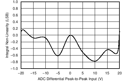
Figure 42 shows a 16-bit, differential, 8-channel, multiplexed, data-acquisition system. This example is typical in industrial applications that require low distortion and a high-voltage differential input. The circuit uses the ADS8864, a 16-bit, 400-kSPS successive-approximation-resistor (SAR) analog-to-digital converter (ADC), along with a precision, high-voltage, signal-conditioning front end, and a 4-channel differential mux. This TI Precision Design details the process for optimizing the precision, high-voltage, front-end drive circuit using the MUX507, OPA192 and OPA140 to achieve excellent dynamic performance and linearity with the ADS8864.
 Figure 42. 16-Bit Precision Multiplexed Data-Acquisition System for High-Voltage Inputs With Lowest Distortion
9.2.1 Design Requirements
The primary objective is to design a ±20 V, differential, 8-channel, multiplexed, data-acquisition system with lowest distortion using the 16-bit ADS8864 at a throughput of 400 kSPS for a 10-kHz, full-scale, pure, sine-wave input. The design requirements for this block design are:
- System supply voltage: ±15 V
- ADC supply voltage: 3.3 V
- ADC sampling rate: 400 kSPS
- ADC reference voltage (REFP): 4.096 V
- System input signal: A high-voltage differential input signal with a peak amplitude of 20 V and frequency (fIN) of 10 kHz are applied to each differential input of the mux.
9.2.2 Detailed Design Procedure
The purpose of this precision design is to design an optimal, high-voltage, multiplexed, data-acquisition system for highest system linearity and fast settling. The overall system block diagram is illustrated in Figure 42. The circuit is a multichannel, data-acquisition signal chain consisting of an input low-pass filter, mux, mux output buffer, attenuating SAR ADC driver, and the reference driver. The architecture allows fast sampling of multiple channels using a single ADC, providing a low-cost solution. This design systematically approaches each analog circuit block to achieve a 16-bit settling for a full-scale input stage voltage and linearity for a 10-kHz sinusoidal input signal at each input channel. Detailed design considerations and component selection procedure can be found in the TI Precision Design TIPD151, 16-Bit, 400-kSPS, 4-Channel Multiplexed Data-Acquisition System for High-Voltage Inputs with Lowest Distortion.
9.2.3 Application Curve
 Figure 43. ADC 16-Bit Linearity Error for the Multiplexed Data-Acquisition Block