JAJSCO7A November 2016 – November 2017 MUX506 , MUX507
PRODUCTION DATA.
- 1 特長
- 2 アプリケーション
- 3 概要
- 4 改訂履歴
- 5 Pin Configuration and Functions
- 6 Specifications
- 7 Parameter Measurement Information
- 8 Detailed Description
- 9 Application and Implementation
- 10Power Supply Recommendations
- 11Layout
- 12デバイスおよびドキュメントのサポート
- 13メカニカル、パッケージ、および注文情報
パッケージ・オプション
メカニカル・データ(パッケージ|ピン)
サーマルパッド・メカニカル・データ
- DW|28
発注情報
11 Layout
11.1 Layout Guidelines
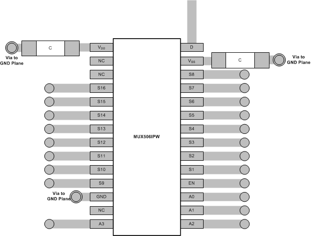
Figure 45 illustrates an example of a PCB layout with the MUX506IPW, and Figure 46 illustrates an example of a PCB layout with MUX507IPW.
Some key considerations are:
- Decouple the VDD and VSS pins with a 0.1-µF capacitor, placed as close to the pin as possible. Make sure that the capacitor voltage rating is sufficient for the VDD and VSS supplies.
- Keep the input lines as short as possible. In case of the differential signal, make sure the A inputs and B inputs are as symmetric as possible.
- Use a solid ground plane to help distribute heat and reduce electromagnetic interference (EMI) noise pickup.
- Do not run sensitive analog traces in parallel with digital traces. Avoid crossing digital and analog traces if possible, and only make perpendicular crossings when necessary.
11.2 Layout Example
 Figure 45. MUX506IPW Layout Example
 Figure 46. MUX507IPW Layout Example