JAJSF79F March 2002 – April 2018 OPA2357 , OPA357
PRODUCTION DATA.
- 1 特長
- 2 アプリケーション
- 3 概要
- 4 改訂履歴
- 5 Pin Configuration and Functions
- 6 Specifications
-
7 Detailed Description
- 7.1 Overview
- 7.2 Functional Block Diagram
- 7.3
Feature Description
- 7.3.1 OPAx357 Comparison
- 7.3.2 Operating Voltage
- 7.3.3 Enable Function
- 7.3.4 Rail-to-Rail Input
- 7.3.5 Rail-to-Rail Output
- 7.3.6 Output Drive
- 7.3.7 Video
- 7.3.8 Wideband Video Multiplexing
- 7.3.9 Driving Analog-to-Digital Converters
- 7.3.10 Capacitive Load and Stability
- 7.3.11 Wideband Transimpedance Amplifier
- 7.4 Device Functional Modes
- 8 Application and Implementation
- 9 Power Supply Recommendations
- 10Layout
- 11デバイスおよびドキュメントのサポート
- 12メカニカル、パッケージ、および注文情報
7.3.10 Capacitive Load and Stability
The OPA357 series of op amps can drive a wide range of capacitive loads. However, all op amps under certain conditions may become unstable. Op amp configuration, gain, and load value are just a few factors to consider when determining stability. An op amp in unity-gain configuration is most susceptible to the effects of capacitive loading. The capacitive load reacts with the op amp output resistance, along with any additional load resistance, to create a pole in the small-signal response that degrades the phase margin; see Figure 14 for details.
The OPA357 topology enhances its ability to drive capacitive loads. In unity gain, these op amps perform well with large capacitive loads. See Figure 15 for details.
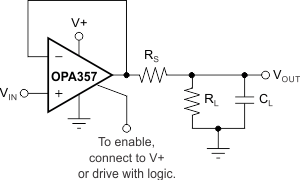
One method of improving capacitive load drive in the unity-gain configuration is to insert a 10-Ω to 20-Ω resistor in series with the output, as shown in Figure 39. This method significantly reduces ringing with large capacitive loads; see Figure 14. However, if there is a resistive load in parallel with the capacitive load, RS creates a voltage divider. This process introduces a DC error at the output and slightly reduces output swing. This error can be insignificant. For instance, with RL = 10 kΩ and RS = 20 Ω, there is only about a 0.2% error at the output.
 Figure 39. Series Resistor in Unity-Gain Configuration Improves Capacitive Load Drive