JAJSS69B September 2000 – April 2024 OPA627 , OPA637
PRODMIX
- 1
- 1 特長
- 2 アプリケーション
- 3 概要
- 4 Pin Configuration and Functions
-
5 Specifications
- 5.1 Absolute Maximum Ratings
- 5.2 ESD Ratings
- 5.3 Recommended Operating Conditions
- 5.4 Thermal Information: OPA627
- 5.5 Thermal Information: OPA637
- 5.6 Electrical Characteristics: OPA627BU, OPA627AU
- 5.7 Electrical Characteristics: OPA627AM, OPA627BM, OPA627SM
- 5.8 Electrical Characteristics: OPA637
- 5.9 Typical Characteristics
- 6 Detailed Description
- 7 Application and Implementation
- 8 Device and Documentation Support
- 9 Revision History
- 10Mechanical, Packaging, and Orderable Information
パッケージ・オプション
メカニカル・データ(パッケージ|ピン)
サーマルパッド・メカニカル・データ
発注情報
6.3.7 Input Protection
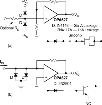
The inputs of the OPA6x7 are protected for voltages from +VS + 0.5V to –VS – 0.5V. If the input voltage can exceed these limits, protect the amplifier by limiting the current into the input pins. The diode clamps shown in (a) in Figure 6-7 prevent the input voltage from exceeding one forward diode voltage drop beyond the power supplies, which is well within the safe limits. If the input source can deliver current in excess of the maximum forward current of the protection diodes, use a series resistor, RS, to limit the current. Be aware that adding resistance to the input increases noise. The 4nV/√Hz theoretical thermal noise of a 1kΩ resistor adds to the 4.5nV/√Hz noise of the OPA6x7 (by the square-root of the sum of the squares), producing a total noise of 6nV/√Hz. Resistors less than 100Ω add negligible noise.
Leakage current in the protection diodes can increase the total input bias current of the circuit. The specified maximum leakage current for commonly used diodes such as the 1N4148 is approximately 25nA, more than a thousand times larger than the input bias current of the OPA6x7. Leakage current of these diodes is typically much lower and can be adequate in many applications. Light falling on the junction of the protection diodes can dramatically increase leakage current, so shield common glass-packaged diodes from ambient light. Very low leakage can be achieved by using a diode-connected FET as shown. The 2N4117A is specified at 1pA and the metal case shields the junction from light.
Sometimes input protection is required on I/V converters of inverting amplifiers; see (b) in Figure 6-7. Although in normal operation, the voltage at the summing junction is near zero (equal to the offset voltage of the amplifier), large input transients can cause this node to exceed 0.5V beyond the power supplies. In this case, protect the summing junction with diode clamps connected to ground. Even with the low voltage present at the summing junction, common signal diodes can have excessive leakage current. Because the reverse voltage on these diodes is clamped, a diode-connected signal transistor can act as an inexpensive low leakage diode; see (b) in Figure 6-7.
 Figure 6-7 Input Protection Circuits