JAJSHS6E August   2019  – August 2024 OPA810

PRODUCTION DATA  

  1.   1
  2. 特長
  3. アプリケーション
  4. 概要
  5. Device Comparison Table
  6. Pin Configuration and Functions
  7. Specifications
    1. 6.1  Absolute Maximum Ratings
    2. 6.2  ESD Ratings
    3. 6.3  Recommended Operating Conditions
    4. 6.4  Thermal Information
    5. 6.5  Electrical Characteristics: 10 V
    6. 6.6  Electrical Characteristics: 24 V
    7. 6.7  Electrical Characteristics: 5 V
    8. 6.8  Typical Characteristics: VS = 10 V
    9. 6.9  Typical Characteristics: VS = 24 V
    10. 6.10 Typical Characteristics: VS = 5 V
    11. 6.11 Typical Characteristics: ±2.375-V to ±12-V Split Supply
  8. Detailed Description
    1. 7.1 Overview
    2. 7.2 Functional Block Diagram
    3. 7.3 Feature Description
      1. 7.3.1 OPA810 Architecture
      2. 7.3.2 ESD Protection
    4. 7.4 Device Functional Modes
      1. 7.4.1 Split-Supply Operation (±2.375 V to ±13.5 V)
      2. 7.4.2 Single-Supply Operation (4.75 V to 27 V)
  9. Application and Implementation
    1. 8.1 Application Information
      1. 8.1.1 Amplifier Gain Configurations
      2. 8.1.2 Selection of Feedback Resistors
      3. 8.1.3 Noise Analysis and the Effect of Resistor Elements on Total Noise
    2. 8.2 Typical Applications
      1. 8.2.1 Transimpedance Amplifier
        1. 8.2.1.1 Design Requirements
        2. 8.2.1.2 Detailed Design Procedure
        3. 8.2.1.3 Application Curves
      2. 8.2.2 High-Z Input Data Acquisition Front-End
      3. 8.2.3 Multichannel Sensor Interface
    3. 8.3 Power Supply Recommendations
    4. 8.4 Layout
      1. 8.4.1 Layout Guidelines
        1. 8.4.1.1 Thermal Considerations
      2. 8.4.2 Layout Example
  10. Device and Documentation Support
    1. 9.1 サード・パーティ製品に関する免責事項
    2. 9.2 Documentation Support
      1. 9.2.1 Related Documentation
    3. 9.3 ドキュメントの更新通知を受け取る方法
    4. 9.4 サポート・リソース
    5. 9.5 Trademarks
    6. 9.6 静電気放電に関する注意事項
    7. 9.7 用語集
  11. 10Revision History
  12. 11Mechanical, Packaging, and Orderable Information

パッケージ・オプション

デバイスごとのパッケージ図は、PDF版データシートをご参照ください。

メカニカル・データ(パッケージ|ピン)
  • D|8
  • DBV|5
  • DCK|5
サーマルパッド・メカニカル・データ
発注情報

Typical Characteristics: VS = 10 V

at VS+ = 5 V, VS– = –5 V, RL = 1 kΩ, input and output are biased to midsupply, and TA ≈ 25°C. For AC specifications, VO = 2 VPP, G = 2 V/V, RF = 1 kΩ, and CL = 4.7 pF (unless otherwise noted)
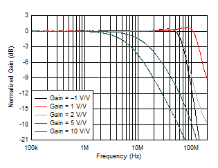
OPA810 Small-Signal Frequency Response vs Gain
See Figure 8-1 and Figure 8-2, VO = 20 mVPP
Figure 6-1 Small-Signal Frequency Response vs Gain
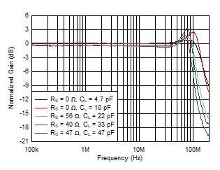
OPA810 Small-Signal Frequency Response vs CL
See Figure 8-1 and Figure 7-1,
VO = 20 mVPP, gain = 1 V/V, RF = 0 Ω
Figure 6-3 Small-Signal Frequency Response vs CL
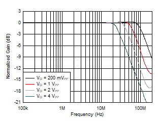
OPA810 Large-Signal Frequency Response vs Output Voltage
See Figure 8-1, gain = 1 V/V, RF = 0 Ω
Figure 6-5 Large-Signal Frequency Response vs Output Voltage
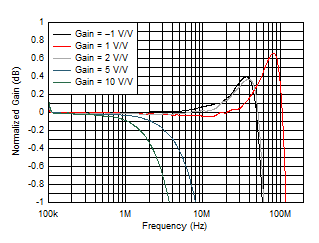
OPA810 Small-Signal Response Flatness vs Gain
See Figure 8-1 and Figure 8-2, VO = 20 mVPP
Figure 6-7 Small-Signal Response Flatness vs Gain
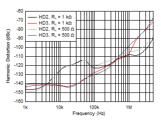
OPA810 Harmonic Distortion vs Frequency
See Figure 8-2, gain = –1 V/V
Figure 6-9 Harmonic Distortion vs Frequency
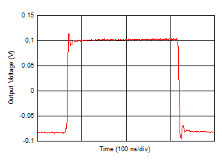
OPA810 Small-Signal Transient Response
See Figure 8-1, gain = 1 V/V, RF = 0 Ω, CL = 10 pF
Figure 6-11 Small-Signal Transient Response
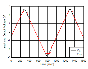
OPA810 Input
                        Overdrive Recovery
See Figure 8-1, gain = 1 V/V, RF = 0 Ω
Figure 6-13 Input Overdrive Recovery
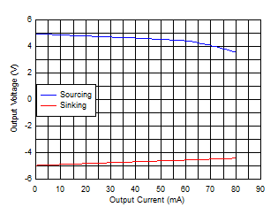
OPA810 Output Voltage vs Load Current
 
Figure 6-15 Output Voltage vs Load Current
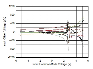
OPA810 Input
                        Offset Voltage vs Input Common-Mode Voltage
Measured for 12 units
Figure 6-17 Input Offset Voltage vs Input Common-Mode Voltage
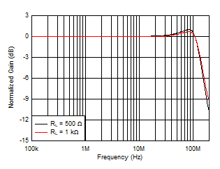
OPA810 Small-Signal Frequency Response vs Output Load
See Figure 8-1, VO = 20 mVPP, gain = 1 V/V, RF = 0 Ω
Figure 6-2 Small-Signal Frequency Response vs Output Load
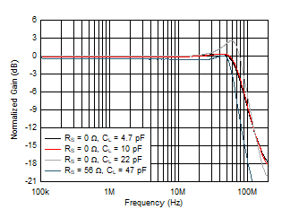
OPA810 Small-Signal Frequency Response vs CL
See Figure 8-1and Figure 7-1, VO = 20 mVPP, gain = 2 V/V
 
Figure 6-4 Small-Signal Frequency Response vs CL
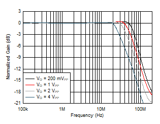
OPA810 Large-Signal Frequency Response vs Output Voltage
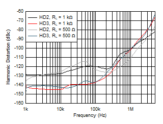
See Figure 8-1, gain = 2 V/V
Figure 6-6 Large-Signal Frequency Response vs Output Voltage
OPA810 Harmonic Distortion vs Frequency
See Figure 8-1, gain = 2 V/V
Figure 6-8 Harmonic Distortion vs Frequency
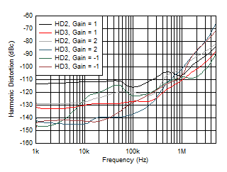
OPA810 Harmonic Distortion vs Gain
See Figure 8-1 and Figure 8-2, RF = 0 Ω
Figure 6-10 Harmonic Distortion vs Gain
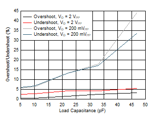
OPA810 Overshoot and Undershoot vs CL
See Figure 8-1, gain = 1 V/V, RF = 0 Ω
Figure 6-12 Overshoot and Undershoot vs CL
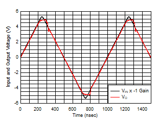
OPA810 Output Overdrive Recovery
See Figure 8-2, gain = –1 V/V
Figure 6-14 Output Overdrive Recovery
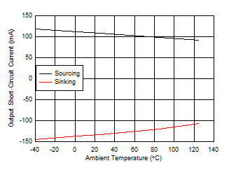
OPA810 Output Short-Circuit Current vs Ambient Temperature
Output saturated and then short-circuited
Figure 6-16 Output Short-Circuit Current vs Ambient Temperature