JAJSHS6E August   2019  – August 2024 OPA810

PRODUCTION DATA  

  1.   1
  2. 特長
  3. アプリケーション
  4. 概要
  5. Device Comparison Table
  6. Pin Configuration and Functions
  7. Specifications
    1. 6.1  Absolute Maximum Ratings
    2. 6.2  ESD Ratings
    3. 6.3  Recommended Operating Conditions
    4. 6.4  Thermal Information
    5. 6.5  Electrical Characteristics: 10 V
    6. 6.6  Electrical Characteristics: 24 V
    7. 6.7  Electrical Characteristics: 5 V
    8. 6.8  Typical Characteristics: VS = 10 V
    9. 6.9  Typical Characteristics: VS = 24 V
    10. 6.10 Typical Characteristics: VS = 5 V
    11. 6.11 Typical Characteristics: ±2.375-V to ±12-V Split Supply
  8. Detailed Description
    1. 7.1 Overview
    2. 7.2 Functional Block Diagram
    3. 7.3 Feature Description
      1. 7.3.1 OPA810 Architecture
      2. 7.3.2 ESD Protection
    4. 7.4 Device Functional Modes
      1. 7.4.1 Split-Supply Operation (±2.375 V to ±13.5 V)
      2. 7.4.2 Single-Supply Operation (4.75 V to 27 V)
  9. Application and Implementation
    1. 8.1 Application Information
      1. 8.1.1 Amplifier Gain Configurations
      2. 8.1.2 Selection of Feedback Resistors
      3. 8.1.3 Noise Analysis and the Effect of Resistor Elements on Total Noise
    2. 8.2 Typical Applications
      1. 8.2.1 Transimpedance Amplifier
        1. 8.2.1.1 Design Requirements
        2. 8.2.1.2 Detailed Design Procedure
        3. 8.2.1.3 Application Curves
      2. 8.2.2 High-Z Input Data Acquisition Front-End
      3. 8.2.3 Multichannel Sensor Interface
    3. 8.3 Power Supply Recommendations
    4. 8.4 Layout
      1. 8.4.1 Layout Guidelines
        1. 8.4.1.1 Thermal Considerations
      2. 8.4.2 Layout Example
  10. Device and Documentation Support
    1. 9.1 サード・パーティ製品に関する免責事項
    2. 9.2 Documentation Support
      1. 9.2.1 Related Documentation
    3. 9.3 ドキュメントの更新通知を受け取る方法
    4. 9.4 サポート・リソース
    5. 9.5 Trademarks
    6. 9.6 静電気放電に関する注意事項
    7. 9.7 用語集
  11. 10Revision History
  12. 11Mechanical, Packaging, and Orderable Information

パッケージ・オプション

デバイスごとのパッケージ図は、PDF版データシートをご参照ください。

メカニカル・データ(パッケージ|ピン)
  • D|8
  • DBV|5
  • DCK|5
サーマルパッド・メカニカル・データ
発注情報

Typical Characteristics: ±2.375-V to ±12-V Split Supply

at VO = 2 VPP, RF = 1 kΩ, RL = 1 kΩ and TA ≈ 25°C (unless otherwise noted)
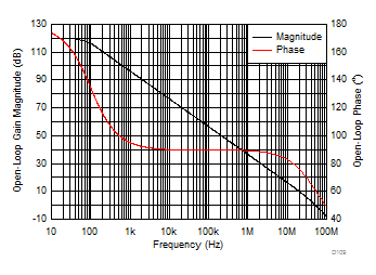
OPA810 Open-Loop Gain and Phase vs Frequency
Simulated with no output load
Figure 6-42 Open-Loop Gain and Phase vs Frequency
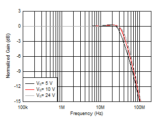
OPA810 Large-Signal Response vs Supply Voltage
See Figure 8-1, gain = 2 V/V
Figure 6-44 Large-Signal Response vs Supply Voltage
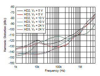
OPA810 Harmonic Distortion vs Frequency vs Supply Voltage
See Figure 8-2, gain = –1 V/V
Figure 6-46 Harmonic Distortion vs Frequency vs Supply Voltage
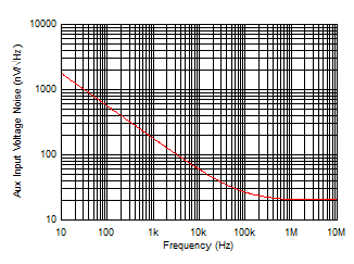
OPA810 Auxiliary Input Stage Voltage Noise Density vs Frequency
Measured then fit to ideal 1/f model
Figure 6-48 Auxiliary Input Stage Voltage Noise Density vs Frequency
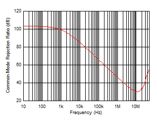
OPA810 Common-Mode Rejection Ratio vs Frequency
VS = 10 V and 24 V
Figure 6-50 Common-Mode Rejection Ratio vs Frequency
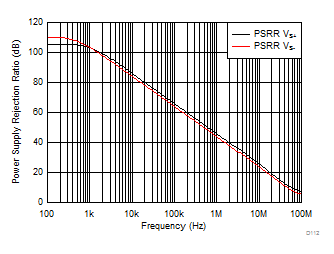
OPA810 Power
                        Supply Rejection Ratio vs Frequency
Simulated curves, VS = 24 V
Figure 6-52 Power Supply Rejection Ratio vs Frequency
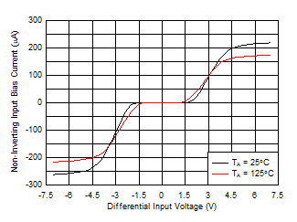
OPA810 Input
                        Bias Current vs Differential Input Voltage
Abs (VIN,Diff (max)) = VS when VS < 7 V
Figure 6-54 Input Bias Current vs Differential Input Voltage
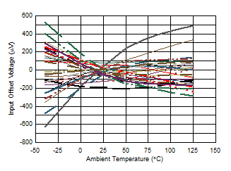
OPA810 Input
                        Offset Voltage vs Ambient Temperature
32 units, SOIC package
Figure 6-56 Input Offset Voltage vs Ambient Temperature
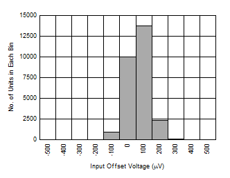
OPA810 Input
                        Offset Voltage Distribution
27000 units, µ = 16 µV, σ = 63 µV, VS = 24 V
Figure 6-58 Input Offset Voltage Distribution
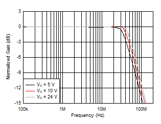
OPA810 Large-Signal Response vs Supply Voltage
See Figure 8-1, gain = 1 V/V, RF = 0 Ω
Figure 6-43 Large-Signal Response vs Supply Voltage
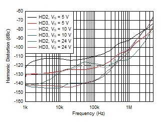
OPA810 Harmonic Distortion vs Frequency vs Supply Voltage
See Figure 8-1, gain = 2 V/V
Figure 6-45 Harmonic Distortion vs Frequency vs Supply Voltage
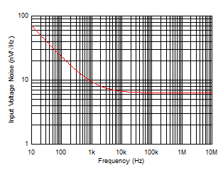
OPA810 Input
                        Voltage Noise Density vs Frequency
Measured then fit to ideal 1/f model
Figure 6-47 Input Voltage Noise Density vs Frequency
OPA810 Open-Loop Output Impedance vs Frequency
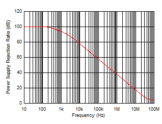
 
Figure 6-49 Open-Loop Output Impedance vs Frequency
OPA810 Power
                        Supply Rejection Ratio vs Frequency
VS = 5 V and 10 V
Figure 6-51 Power Supply Rejection Ratio vs Frequency
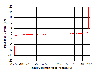
OPA810 Input
                        Bias Current vs Input Common-Mode Voltage
VS = ±12 V
Figure 6-53 Input Bias Current vs Input Common-Mode Voltage
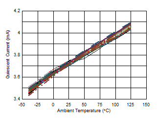
OPA810 Quiescent Current vs Ambient Temperature
32 units, SOIC package, VS = ±5 V
Figure 6-55 Quiescent Current vs Ambient Temperature
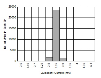
OPA810 Quiescent Current Distribution
27000 units, µ = 3.82 mA, σ = 17 µA, VS = 24 V
Figure 6-57 Quiescent Current Distribution
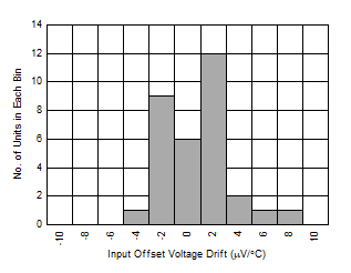
OPA810 Input
                        Offset Voltage Drift Distribution
–40°C to +125°C fit, 32 units, µ = –0.15 µV/°C, σ = 2.5 µV/°C
Figure 6-59 Input Offset Voltage Drift Distribution