JAJSOP2 December 2022 OPT3005
PRODUCTION DATA
- 1 特長
- 2 アプリケーション
- 3 概要
- 4 Revision History
- 5 概要 (続き)
- 6 Pin Configuration and Functions
- 7 Specifications
-
8 Detailed Description
- 8.1 Overview
- 8.2 Functional Block Diagram
- 8.3 Feature Description
- 8.4 Device Functional Modes
- 8.5 Programming
- 8.6
Register Maps
- 8.6.1
Internal Registers
- 8.6.1.1
Register Descriptions
- 8.6.1.1.1 Result Register (offset = 00h)
- 8.6.1.1.2 Configuration Register (offset = 01h) [reset = C810h]
- 8.6.1.1.3 Low-Limit Register (offset = 02h) [reset = C0000h]
- 8.6.1.1.4 High-Limit Register (offset = 03h) [reset = BFFFh]
- 8.6.1.1.5 Manufacturer ID Register (offset = 7Eh) [reset = 5449h]
- 8.6.1.1.6 Device ID Register (offset = 7Fh) [reset = 3001h]
- 8.6.1.1
Register Descriptions
- 8.6.1
Internal Registers
- 9 Application and Implementation
- 10Device and Documentation Support
- 11Mechanical, Packaging, and Orderable Information
9.5.4 Mechanical Drawings
Identifying Package Orientation Using Automated Optical Inspection (AOI) Systems
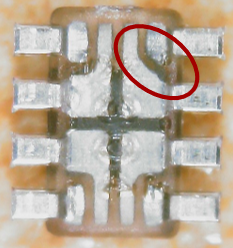
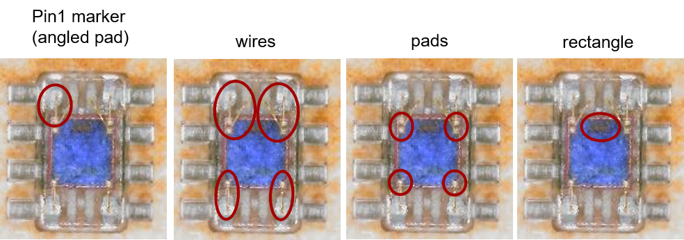
Automated optical inspection (AOI) systems are used in the PCB assembly process to identify the device orientation during device placement. Typically, on non-optical packages, the pin 1 marker is a white dot or indentation on the black package. This is used by the AOI system to orient the package. Light sensor ICs such as OPT3005 utilize a transparent package to allow light to enter the package and reach the sensor. This section provides instruction for determining orientation on the package. The following figures show how the package can be oriented from the bottom and top side. On the bottom side the package has a pin 1 identifier. On the top side there are four features that can be used to orient the device. 1) the pin 1 identifier can be seen through the package. 2) and 3) the bond wires and bond pads on the die can also be used. The asymmetry in either wires or pads (4 at the top and 2 at the bottom) can be used to orient the device. 4) the rectangular feature on the die indicates orientation.
 Figure 9-8 Identifying Package Orientation -
Backside
 Figure 9-9 Identifying Package Orientation -
Topside