JAJSOP2 December   2022 OPT3005

PRODUCTION DATA  

  1. 特長
  2. アプリケーション
  3. 概要
  4. Revision History
  5. 概要 (続き)
  6. Pin Configuration and Functions
  7. Specifications
    1. 7.1 Absolute Maximum Ratings
    2. 7.2 ESD Ratings
    3. 7.3 Recommended Operating Conditions
    4. 7.4 Thermal Information
    5. 7.5 Electrical Characteristics
    6. 7.6 Timing Requirements
    7. 7.7 Typical Characteristics
  8. Detailed Description
    1. 8.1 Overview
    2. 8.2 Functional Block Diagram
    3. 8.3 Feature Description
      1. 8.3.1 Human Eye Matching
      2. 8.3.2 Automatic Full-Scale Range Setting
      3. 8.3.3 Interrupt Operation, INT Pin, and Interrupt Reporting Mechanisms
      4. 8.3.4 I2C Bus Overview
        1. 8.3.4.1 Serial Bus Address
        2. 8.3.4.2 Serial Interface
    4. 8.4 Device Functional Modes
      1. 8.4.1 Automatic Full-Scale Setting Mode
      2. 8.4.2 Interrupt Reporting Mechanism Modes
        1. 8.4.2.1 Latched Window-Style Comparison Mode
        2. 8.4.2.2 Transparent Hysteresis-Style Comparison Mode
        3. 8.4.2.3 End-of-Conversion Mode
        4. 8.4.2.4 End-of-Conversion and Transparent Hysteresis-Style Comparison Mode
    5. 8.5 Programming
      1. 8.5.1 Writing and Reading
        1. 8.5.1.1 High-Speed I2C Mode
        2. 8.5.1.2 General-Call Reset Command
        3. 8.5.1.3 SMBus Alert Response
    6. 8.6 Register Maps
      1. 8.6.1 Internal Registers
        1. 8.6.1.1 Register Descriptions
          1. 8.6.1.1.1 Result Register (offset = 00h)
          2. 8.6.1.1.2 Configuration Register (offset = 01h) [reset = C810h]
          3. 8.6.1.1.3 Low-Limit Register (offset = 02h) [reset = C0000h]
          4. 8.6.1.1.4 High-Limit Register (offset = 03h) [reset = BFFFh]
          5. 8.6.1.1.5 Manufacturer ID Register (offset = 7Eh) [reset = 5449h]
          6. 8.6.1.1.6 Device ID Register (offset = 7Fh) [reset = 3001h]
  9. Application and Implementation
    1. 9.1 Application Information
      1. 9.1.1 Electrical Interface
      2. 9.1.2 Optical Interface
    2. 9.2 Typical Application
      1. 9.2.1 Design Requirements
      2. 9.2.2 Detailed Design Procedure
        1. 9.2.2.1 Optomechanical Design
        2. 9.2.2.2 Dark Window Selection and Compensation
      3. 9.2.3 Application Curves
    3. 9.3 Do's and Don'ts
    4. 9.4 Power-Supply Recommendations
    5. 9.5 Layout
      1. 9.5.1 Layout Guidelines
      2. 9.5.2 Layout Example
      3. 9.5.3 Soldering and Handling Recommendations
      4. 9.5.4 Mechanical Drawings
  10. 10Device and Documentation Support
    1. 10.1 Documentation Support
      1. 10.1.1 Related Documentation
    2. 10.2 ドキュメントの更新通知を受け取る方法
    3. 10.3 サポート・リソース
    4. 10.4 Trademarks
    5. 10.5 静電気放電に関する注意事項
    6. 10.6 用語集
  11. 11Mechanical, Packaging, and Orderable Information

パッケージ・オプション

メカニカル・データ(パッケージ|ピン)
サーマルパッド・メカニカル・データ
発注情報

Pin Configuration and Functions

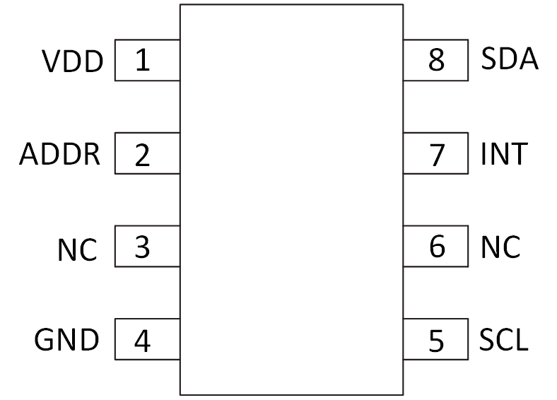
GUID-432CEB60-5A7F-41FB-8074-225BE428C2A4-low.gif Figure 6-1 DTS Package, 8-Pin SOT-5X3, Top View
Table 6-1 Pin Functions
PIN TYPE DESCRIPTION
NO. NAME
1 VDD Power Device power. Connect to a 1.6-V to 3.6-V supply.
2 ADDR Digital input Address pin. This pin sets the LSBs of the I2C address.
3 NC No Connection No Connection
4 GND Power Ground
5 SCL Digital input I2C clock. Connect with a 10-kΩ resistor to a 1.6-V to 5.5-V supply.
6 NC No Connection No Connection
7 INT Digital output Interrupt output open-drain. Connect with a 10-kΩ resistor to a 1.6-V to 5.5-V supply.
8 SDA Digital I/O I2C data. Connect with a 10-kΩ resistor to a 1.6-V to 5.5-V supply.