JAJSDR9 August 2017 OPT3007
PRODUCTION DATA.
- 1 特長
- 2 アプリケーション
- 3 概要
- 4 改訂履歴
- 5 Pin Configuration and Functions
- 6 Specifications
-
7 Detailed Description
- 7.1 Overview
- 7.2 Functional Block Diagram
- 7.3 Feature Description
- 7.4 Device Functional Modes
- 7.5 Programming
- 7.6
Register Maps
- 7.6.1
Internal Registers
- 7.6.1.1
Register Descriptions
- 7.6.1.1.1 Result Register (Offset = 00h)
- 7.6.1.1.2 Configuration Register (Offset = 01h) [Reset = C810h]
- 7.6.1.1.3 Low-Limit Register (Offset = 02h) [Reset = C0000h]
- 7.6.1.1.4 High-Limit Register (Offset = 03h) [Reset = BFFFh]
- 7.6.1.1.5 Manufacturer ID Register (Offset = 7Eh) [Reset = 5449h]
- 7.6.1.1.6 Device ID Register (Offset = 7Fh) [Reset = 3001h]
- 7.6.1.1
Register Descriptions
- 7.6.1
Internal Registers
- 8 Application and Implementation
- 9 Power-Supply Recommendations
- 10Layout
- 11デバイスおよびドキュメントのサポート
- 12メカニカル、パッケージ、および注文情報
10 Layout
10.1 Layout Guidelines
The PCB layout design for the OPT3007 requires a couple of considerations. The design of the cutout to allow light to illuminate the sensor is a critical part of this design. See the Optomechanical Design section for a more detailed discussion of creating this cutout.
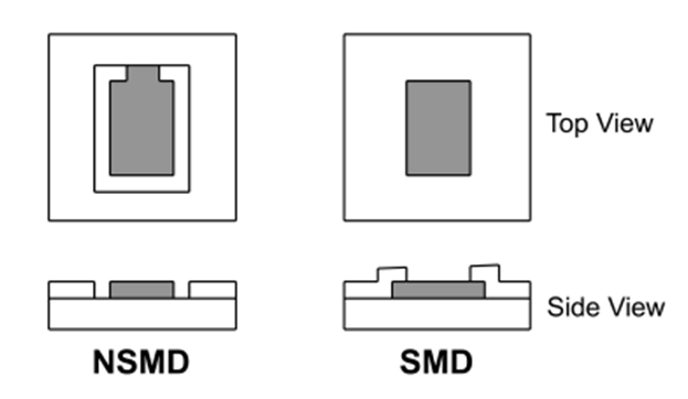
The device layout is also critical for optimal SMT assembly. Two types of land pattern pads can be used for this package: solder mask defined pads (SMD) and non-solder mask defined pads (NSMD). SMD pads have a solder mask opening that is smaller than the metal pads, whereas NSMD has a solder mask opening that is larger than the metal pad.Figure 33 illustrates these types of landing-pattern pads. SMD is preferred because it provides a more accurate soldering-pad dimension with the trace connections. For further discussion of SMT and PCB recommendations, see the Soldering and Handling Recommendations section.
 Figure 33. Soldermask Defined Pad (SMD) and Non-Soldermask Defined Pad (NSMD)
Stabilize the power supply with a capacitor placed close to the OPT3007 VDD and GND pins. Note that optically reflective surfaces of components also affect the performance of the design. The three-dimensional geometry of all components and structures around the sensor must be taken into consideration to prevent unexpected results from secondary optical reflections. Placing capacitors and components at a distance of at least twice the height of the component is usually sufficient, although further placement can still achieve good results. The most optimal optical layout is to place all close components on the opposite side of the PCB from the OPT3007. However, this approach may not be practical for the constraints of every design.
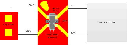
An example PCB layout with the OPT3007 is shown in Figure 35.
10.2 Soldering and Handling Recommendations
The OPT3007 is a very small device with special soldering and handling considerations. See Optomechanical Design for implications of alignment between the device and the cutout area. See Layout Guidelines for considerations of the soldering pads.
As with most optical devices, handle the OPT3007 with special care to make sure optical surfaces stay clean and free from damage. See the Do's and Don'ts section for more detailed recommendations. For best optical performance, clean solder flux and any other possible debris after soldering processes.
10.2.1 Solder Paste
For solder-paste deposition, use a stencil-printing process that involves the transfer of solder paste through predefined apertures with the application of pressure. Stencil parameters, such as aperture area ratio and fabrication process, have a significant impact on paste deposition. Cut the stencil apertures using a laser with an electropolish-fabrication method. Taper the stencil aperture walls by 5° to facilitate paste release. Shifting the solder-paste towards the outside of the device minimizes the possibility of solder getting into the device sensing area. See the mechanical packages attached to the end of this data sheet.
Use solder paste selection type 4 or higher, no-clean, lead-free solder paste. If solder splatters in the reflow process, choose a solder paste with normal- or low-flux contents, or alter the reflow profile per the Reflow Profile section.
10.2.2 Package Placement
Use a pick-and-place nozzle with a size number larger than 0.6 mm. If the placement method is done by programming the component thickness, add 0.04 mm to the actual component thickness so that the package sits halfway into the solder paste. If placement is by force, then choose minimum force no larger than 3N in order to avoid forcing out solder paste, or free falling the package, and to avoid soldering problems such as bridging and solder balling.
10.2.3 Reflow Profile
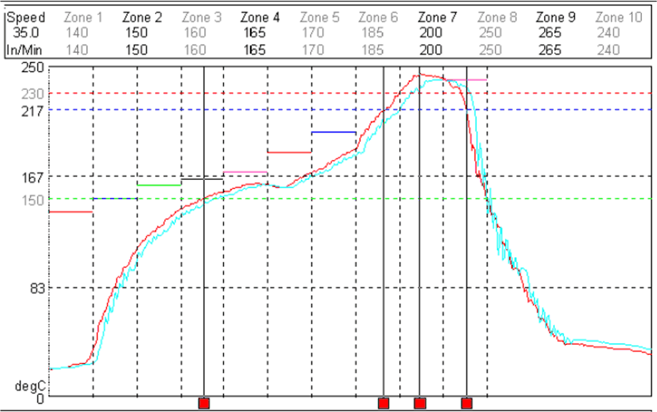
Use the profile in Figure 34, and adjust if necessary. Use a slow solder reflow ramp rate of 1°C to 1.2°C/s to minimize chances of solder splattering onto the sensing area.
 Figure 34. Recommended Solder Reflow Temperature Profile
10.2.4 Special Flexible Printed-Circuit Board (FPCB) Recommendations
Special flexible printed-circuit board (FPCB) design recommendations include:
- Fabricate per IPC-6013.
- Use material of flexible copper clad per IPC 4204/11 (Define polyimide and copper thickness per product application).
- Finish: All exposed copper will be electroless Ni immersion gold (ENIG) per IPC 4556.
- Solder mask per IPC SM840.
- Use a laser to create the cutout for light sensing for better accuracy, and to avoid affecting the soldering pad dimension. Other options, such as punched cutouts, are possible. See the Optomechanical Design section for further discussion ranging from the implications of the device to cutout region size and alignment. The full design must be considered, including the tolerances.
To assist the handling of the very thin flexible circuit, design and fabricate a fixture to hold the flexible circuit through the paste-printing, pick-and-place, and reflow processes. Contact the factory for examples of such fixtures.
10.2.5 Rework Process
If the OPT3007 must be removed from a PCB, discard the device and do not reattach. To remove the package from the PCB/Flexi cable, heat the solder joints above liquidus temperature. Bake the board at 125°C for 4 hours prior to rework to remove moisture that may crack the PCB or causing delamination. Use a thermal heating profile to remove a package that is close to the profile that mounts the package. Clean the site to remove any excess solder and residue to prepare for installing a new package. Use a mini stencil (localized stencil) to apply solder paste to the land pattern. In case a mini stencil cannot be used because of spacing or other reasons, apply solder paste on the package pads directly, then mount, and reflow.
10.3 Layout Example
