JAJSJ77 June   2023 OPT4060

PRODUCTION DATA  

  1.   1
  2. 特長
  3. アプリケーション
  4. 概要
  5. Revision History
  6. 概要 (続き)
  7. Pin Configuration and Functions
  8. Specifications
    1. 7.1 Absolute Maximum Ratings
    2. 7.2 ESD Ratings
    3. 7.3 Recommended Operating Conditions
    4. 7.4 Thermal Information
    5. 7.5 Electrical Characteristics
    6. 7.6 Typical Characteristics
  9. Detailed Description
    1. 8.1 Overview
    2. 8.2 Functional Block Diagram
    3. 8.3 Feature Description
      1. 8.3.1 Infrared Light Rejection
      2. 8.3.2 Automatic Full-Scale Range Setting
      3. 8.3.3 Output Register CRC and Counter
        1. 8.3.3.1 Output Sample Counter
        2. 8.3.3.2 Output CRC
        3. 8.3.3.3 Threshold Detection
    4. 8.4 Device Functional Modes
      1. 8.4.1 Modes of Operation
      2. 8.4.2 Interrupt Modes of Operation
      3. 8.4.3 Light Range Selection
      4. 8.4.4 Selecting Conversion Time
      5. 8.4.5 Light and Color Measurement
        1. 8.4.5.1 Determining ADC Codes for Each Channel
        2. 8.4.5.2 Lux and Color Calculations
        3. 8.4.5.3 Threshold Detection Calculations
      6. 8.4.6 Light Resolution
    5. 8.5 Programming
      1. 8.5.1 I2C Bus Overview
        1. 8.5.1.1 Serial Bus Address
        2. 8.5.1.2 Serial Interface
      2. 8.5.2 Writing and Reading
        1. 8.5.2.1 High-Speed I2C Mode
        2. 8.5.2.2 Burst Read Mode
        3. 8.5.2.3 General-Call Reset Command
        4. 8.5.2.4 SMBus Alert Response
    6. 8.6 Register Maps
      1. 8.6.1 Register Map
  10. Application and Implementation
    1. 9.1 Application Information
    2. 9.2 Typical Application
      1. 9.2.1 Electrical Interface
        1. 9.2.1.1 Design Requirements
          1. 9.2.1.1.1 Optical Interface
        2. 9.2.1.2 Detailed Design Procedure
          1. 9.2.1.2.1 Optomechanical Design
        3. 9.2.1.3 Application Curve
    3. 9.3 Best Design Practices
    4. 9.4 Power Supply Recommendations
    5. 9.5 Layout
      1. 9.5.1 Layout Guidelines
      2. 9.5.2 Layout Example
      3. 9.5.3 Soldering and Handling Recommendations
  11. 10Device and Documentation Support
    1. 10.1 Documentation Support
      1. 10.1.1 Related Documentation
    2. 10.2 ドキュメントの更新通知を受け取る方法
    3. 10.3 サポート・リソース
    4. 10.4 Trademarks
    5. 10.5 静電気放電に関する注意事項
    6. 10.6 用語集
  12. 11Mechanical, Packaging, and Orderable Information

パッケージ・オプション

メカニカル・データ(パッケージ|ピン)
サーマルパッド・メカニカル・データ
発注情報

Soldering and Handling Recommendations

Soldering temperature profile and guidelines are published in future revisions of this document.

As with most optical devices, handle the OPT4060 with special care to ensure optical surfaces stay clean and free from damage. See Best Design Practices for more detailed recommendations. For best optical performance, solder flux and any other possible debris must be cleaned after soldering processes.
GUID-20221207-SS0I-RHKR-WPGK-K57XJ8WQRW2X-low.png
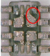
Note: The bottom side of the device features an angled feature to denote the PIN 1
Figure 9-5 Identification Feature for PIN 1
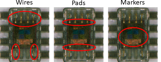
GUID-20221207-SS0I-LP23-2SFQ-FXD19RHSBWVS-low.png Figure 9-6 Identification Features for PIN 1 on Package