JAJS199E April   2003  – July 2019 PCM1753 , PCM1754 , PCM1755

PRODUCTION DATA.  

  1. 特長
  2. アプリケーション
  3. 概要
    1.     Device Images
      1.      機能ブロック図
  4. 改訂履歴
  5. Device Comparison Table
  6. Pin Configuration and Functions
    1.     Pin Functions
  7. Specifications
    1. 7.1 Absolute Maximum Ratings
    2. 7.2 ESD Ratings
    3. 7.3 Recommended Operating Conditions
    4. 7.4 Thermal Information
    5. 7.5 Electrical Characteristics
    6. 7.6 System Clock Input Timing
    7. 7.7 Audio Interface Timing
    8. 7.8 Control Interface Timing Requirements
    9. 7.9 Typical Characteristics
      1. 7.9.1 Digital Filter (De-Emphasis Off)
      2. 7.9.2 Analog Dynamic Performance (Supply Voltage Characteristics)
      3. 7.9.3 Analog Dynamic Performance (Temperature Characteristics)
  8. Detailed Description
    1. 8.1 Overview
    2. 8.2 Functional Block Diagram
    3. 8.3 Feature Description
      1. 8.3.1 System Clock and Reset Functions
        1. 8.3.1.1 System Clock Input
        2. 8.3.1.2 Power-On Reset Functions
      2. 8.3.2 Audio Serial Interface
        1. 8.3.2.1 Audio Data Formats and Timing
      3. 8.3.3 Zero Flag (PCM1754)
      4. 8.3.4 Zero Flag (PCM1753)
      5. 8.3.5 Zero Flag Outputs
      6. 8.3.6 Analog Outputs
        1. 8.3.6.1 VCOM Output
    4. 8.4 Device Functional Modes
      1. 8.4.1 Hardware Control (PCM1754)
      2. 8.4.2 Oversampling Rate Control (PCM1754)
    5. 8.5 Programming
      1. 8.5.1 Software Control (PCM1753/55)
        1. 8.5.1.1 Register Write Operation
    6. 8.6 Register Maps
      1. 8.6.1 Mode Control Registers (PCM1753/55)
        1. 8.6.1.1 User-Programmable Mode Controls
        2. 8.6.1.2 Register Definitions
          1. 8.6.1.2.1  ATx[7:0]: Digital Attenuation Level Setting
          2. 8.6.1.2.2  MUTx: Soft Mute Control
          3. 8.6.1.2.3  OVER: Oversampling Rate Control
          4. 8.6.1.2.4  SRST: Reset
          5. 8.6.1.2.5  DACx: DAC Operation Control
          6. 8.6.1.2.6  DM12: Digital De-Emphasis Function Control
          7. 8.6.1.2.7  DMF[1:0]: Sampling Frequency Selection for the De-Emphasis Function
          8. 8.6.1.2.8  FMT[2:0]: Audio Interface Data Format
          9. 8.6.1.2.9  FLT: Digital Filter Rolloff Control
          10. 8.6.1.2.10 DREV: Output Phase Select
          11. 8.6.1.2.11 ZREV: Zero Flag Polarity Select
          12. 8.6.1.2.12 AZRO: Zero Flag Function Select
  9. Application and Implementation
    1. 9.1 Application Information
    2. 9.2 Typical Application
      1. 9.2.1 Design Requirements
        1. 9.2.1.1 Design Parameters
        2. 9.2.1.2 Power Supplies and Grounding
        3. 9.2.1.3 D/A Output Filter Circuits
      2. 9.2.2 Detailed Design Procedure
        1. 9.2.2.1 Total Harmonic Distortion + Noise
        2. 9.2.2.2 Dynamic Range
        3. 9.2.2.3 Idle Channel Signal-to-Noise Ratio (SNR)
      3. 9.2.3 Application Curves
  10. 10Power Supply Recommendations
  11. 11Layout
    1. 11.1 Layout Guidelines
    2. 11.2 Layout Example
  12. 12デバイスおよびドキュメントのサポート
    1. 12.1 関連資料
    2. 12.2 関連リンク
    3. 12.3 ドキュメントの更新通知を受け取る方法
    4. 12.4 コミュニティ・リソース
    5. 12.5 商標
    6. 12.6 静電気放電に関する注意事項
    7. 12.7 Glossary
  13. 13メカニカル、パッケージ、および注文情報

パッケージ・オプション

メカニカル・データ(パッケージ|ピン)
サーマルパッド・メカニカル・データ
発注情報

Power-On Reset Functions

The PCM175x devices include a power-on reset function. Figure 21 shows the operation of this function. With the system clock active and VCC > 3 V (typical, 2.2 V to 3.7 V), the power-on reset function is enabled. The initialization sequence requires 1024 system clocks from the time VCC > 3 V (typical, 2.2 V to 3.7 V).

During the reset period (1024 system clocks), the analog output is forced to the bipolar zero level, or VCC/2. After the reset period, an internal register is initialized in the next 1/fS period and if SCK, BCK, and LRCK are provided continuously, the PCM175x devices provide proper analog output with unit group delay against the input data.
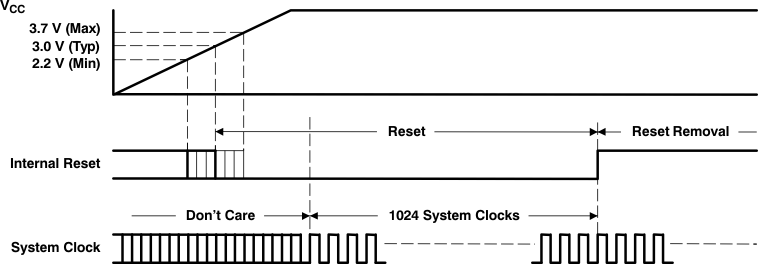
PCM1753 PCM1754 PCM1755 power_on_reset_timing_les254.gifFigure 21. Power-On Reset Timing