JAJS199E April   2003  – July 2019 PCM1753 , PCM1754 , PCM1755

PRODUCTION DATA.  

  1. 特長
  2. アプリケーション
  3. 概要
    1.     Device Images
      1.      機能ブロック図
  4. 改訂履歴
  5. Device Comparison Table
  6. Pin Configuration and Functions
    1.     Pin Functions
  7. Specifications
    1. 7.1 Absolute Maximum Ratings
    2. 7.2 ESD Ratings
    3. 7.3 Recommended Operating Conditions
    4. 7.4 Thermal Information
    5. 7.5 Electrical Characteristics
    6. 7.6 System Clock Input Timing
    7. 7.7 Audio Interface Timing
    8. 7.8 Control Interface Timing Requirements
    9. 7.9 Typical Characteristics
      1. 7.9.1 Digital Filter (De-Emphasis Off)
      2. 7.9.2 Analog Dynamic Performance (Supply Voltage Characteristics)
      3. 7.9.3 Analog Dynamic Performance (Temperature Characteristics)
  8. Detailed Description
    1. 8.1 Overview
    2. 8.2 Functional Block Diagram
    3. 8.3 Feature Description
      1. 8.3.1 System Clock and Reset Functions
        1. 8.3.1.1 System Clock Input
        2. 8.3.1.2 Power-On Reset Functions
      2. 8.3.2 Audio Serial Interface
        1. 8.3.2.1 Audio Data Formats and Timing
      3. 8.3.3 Zero Flag (PCM1754)
      4. 8.3.4 Zero Flag (PCM1753)
      5. 8.3.5 Zero Flag Outputs
      6. 8.3.6 Analog Outputs
        1. 8.3.6.1 VCOM Output
    4. 8.4 Device Functional Modes
      1. 8.4.1 Hardware Control (PCM1754)
      2. 8.4.2 Oversampling Rate Control (PCM1754)
    5. 8.5 Programming
      1. 8.5.1 Software Control (PCM1753/55)
        1. 8.5.1.1 Register Write Operation
    6. 8.6 Register Maps
      1. 8.6.1 Mode Control Registers (PCM1753/55)
        1. 8.6.1.1 User-Programmable Mode Controls
        2. 8.6.1.2 Register Definitions
          1. 8.6.1.2.1  ATx[7:0]: Digital Attenuation Level Setting
          2. 8.6.1.2.2  MUTx: Soft Mute Control
          3. 8.6.1.2.3  OVER: Oversampling Rate Control
          4. 8.6.1.2.4  SRST: Reset
          5. 8.6.1.2.5  DACx: DAC Operation Control
          6. 8.6.1.2.6  DM12: Digital De-Emphasis Function Control
          7. 8.6.1.2.7  DMF[1:0]: Sampling Frequency Selection for the De-Emphasis Function
          8. 8.6.1.2.8  FMT[2:0]: Audio Interface Data Format
          9. 8.6.1.2.9  FLT: Digital Filter Rolloff Control
          10. 8.6.1.2.10 DREV: Output Phase Select
          11. 8.6.1.2.11 ZREV: Zero Flag Polarity Select
          12. 8.6.1.2.12 AZRO: Zero Flag Function Select
  9. Application and Implementation
    1. 9.1 Application Information
    2. 9.2 Typical Application
      1. 9.2.1 Design Requirements
        1. 9.2.1.1 Design Parameters
        2. 9.2.1.2 Power Supplies and Grounding
        3. 9.2.1.3 D/A Output Filter Circuits
      2. 9.2.2 Detailed Design Procedure
        1. 9.2.2.1 Total Harmonic Distortion + Noise
        2. 9.2.2.2 Dynamic Range
        3. 9.2.2.3 Idle Channel Signal-to-Noise Ratio (SNR)
      3. 9.2.3 Application Curves
  10. 10Power Supply Recommendations
  11. 11Layout
    1. 11.1 Layout Guidelines
    2. 11.2 Layout Example
  12. 12デバイスおよびドキュメントのサポート
    1. 12.1 関連資料
    2. 12.2 関連リンク
    3. 12.3 ドキュメントの更新通知を受け取る方法
    4. 12.4 コミュニティ・リソース
    5. 12.5 商標
    6. 12.6 静電気放電に関する注意事項
    7. 12.7 Glossary
  13. 13メカニカル、パッケージ、および注文情報

パッケージ・オプション

メカニカル・データ(パッケージ|ピン)
サーマルパッド・メカニカル・データ
発注情報

Dynamic Range

Dynamic range is specified as A-weighted THD+N measured with a –60-dB full-scale, 1-kHz digital sine wave stimulus at the input of the D/A converter. This measurement is designed to give a good indicator of how the DAC performs given a low-level input signal.

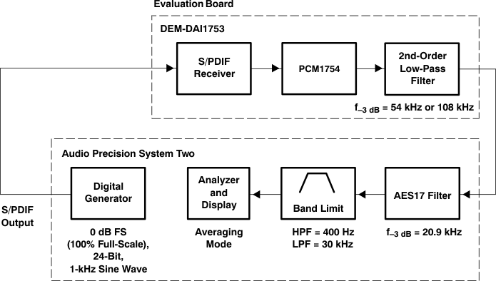
The measurement setup for the dynamic range measurement is shown in Figure 34, and is similar to the THD+N test setup discussed previously. The differences include the band limit filter selection, the additional A-weighting filter, and the –60-dB full-scale input level.
PCM1753 PCM1754 PCM1755 test_setup_thdn_les254.gifFigure 33. Test Setup for THD+N Measurement