-
PCM1802 Single-Ended Analog-Input 24-Bit, 96-kHz Stereo A/D Converter
- 1 Features
- 2 Applications
- 3 Description
- 4 Revision History
- 5 Pin Configuration and Functions
-
6 Specifications
- 6.1 Absolute Maximum Ratings
- 6.2 ESD Ratings
- 6.3 Recommended Operating Conditions
- 6.4 Thermal Information
- 6.5 Electrical Characteristics
- 6.6 Typical Characteristics
- 7 Detailed Description
- 8 Application and Implementation
- 9 Power Supply Recommendations
- 10Layout
- 11Device and Documentation Support
- 12Mechanical, Packaging, and Orderable Information
- IMPORTANT NOTICE
PCM1802 Single-Ended Analog-Input 24-Bit, 96-kHz Stereo A/D Converter
1 Features
- 24-Bit Delta-Sigma Stereo A/D Converter
- Single-Ended Voltage Input: 3 VP–P
- Antialiasing Filter Included
- Oversampling Decimation Filter
- Oversampling Frequency: ×64, ×128
- Pass-Band Ripple: ±0.05 dB
- Stop-Band Attenuation: –65 dB
- On-Chip High-Pass Filter: 0.84 Hz (44.1 kHz)
- High Performance
- THD+N: 96 dB (Typical)
- SNR: 105 dB (Typical)
- Dynamic Range: 105 dB (Typical)
- PCM Audio Interface
- Master and Slave Mode Selectable
- Data Formats: 24-Bit Left-Justified; 24-Bit I2S; 20-bit or 24-Bit Right-Justified
- Sampling Rate: 16 kHz to 96 kHz
- System Clock: 256 fS, 384 fS, 512 fS, 768 fS
- Dual Power Supplies: 5 V (Analog), 3.3 V (Digital)
- Package: 20-Pin SSOP
2 Applications
- AV Amplifier Receivers
- MD Players
- CD Recorders
- Multitrack Receivers
- Electric Musical Instruments
3 Description
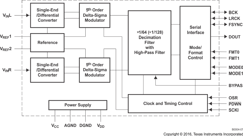
The PCM1802 is a high-performance, low-cost, single-chip stereo analog-to-digital converter with single-ended analog voltage input. The PCM1802 uses a delta-sigma modulator with 64-times or 128‑times oversampling, and includes a digital decimation filter and high-pass filter (HPF), which removes the DC component of the input signal. For various applications, the PCM1802 supports master and slave modes and four data formats in serial interface. The PCM1802 is suitable for a wide variety of cost-sensitive consumer applications where good performance, 5-V analog supply, and 3.3-V digital supply operation is required. The PCM1802 is fabricated using a highly advanced CMOS process and is available in the DB 20-pin SSOP package.
Device Information(1)
| PART NUMBER | PACKAGE | BODY SIZE (NOM) |
|---|---|---|
| PCM1802 | SSOP (20) | 7.20 mm × 5.30 mm |
- For all available packages, see the orderable addendum at the end of the data sheet.
Block Diagram
4 Revision History
Changes from C Revision (January 2005) to D Revision
- Added ESD Ratings table, Feature Description section, Device Functional Modes, Application and Implementation section, Power Supply Recommendations section, Layout section, Device and Documentation Support section, and Mechanical, Packaging, and Orderable Information section.Go
- Deleted Lead temperature (soldering), 260°C for 5 s, from Absolute Maximum Ratings tableGo
- Added Thermal Information tableGo
- Changed Thermal resistance, RθJA, value in Thermal Information table From: 115°C/W To: 80.8°C/WGo
5 Pin Configuration and Functions
Pin Functions
| PIN | I/O | DESCRIPTION | |
|---|---|---|---|
| NAME | NO. | ||
| AGND | 6 | — | Analog GND |
| BCK | 11 | I/O | Bit clock input and output(1) |
| BYPAS | 8 | I | HPF bypass control. Low: normal mode (DC cut); High: bypass mode (through)(2) |
| DGND | 13 | — | Digital GND |
| DOUT | 12 | O | Audio data output |
| FMT0 | 17 | I | Audio data format select 0 (see Data Format)(2) |
| FMT1 | 18 | I | Audio data format select 1 (see Data Format)(2) |
| FSYNC | 9 | I/O | Frame synchronous clock input and output(1) |
| LRCK | 10 | I/O | Sampling clock input and output(1) |
| MODE0 | 19 | I | Mode select 0 (see Interface Mode)(2) |
| MODE1 | 20 | I | Mode select 1 (see Interface Mode)(2) |
| OSR | 16 | I | Oversampling ratio select. Low: ×64 fS; High: ×128 fS(2) |
| PDWN | 7 | I | Power-down control, active-low(2) |
| SCKI | 15 | I | System clock input; 256 fS, 384 fS, 512 fS, or 768 fS(3) |
| VCC | 5 | — | Analog power supply, 5 V |
| VDD | 14 | — | Digital power supply, 3.3 V |
| VINL | 1 | I | Analog input, L-channel |
| VINR | 2 | I | Analog input, R-channel |
| VREF1 | 3 | — | Reference-1 decoupling capacitor |
| VREF2 | 4 | — | Reference-2 voltage input, normally connected to VCC |
6 Specifications
6.1 Absolute Maximum Ratings
over operating free-air temperature range (unless otherwise noted)(1)| MIN | MAX | UNIT | ||
|---|---|---|---|---|
| Supply voltage | VCC | 6.5 | V | |
| VDD | 4 | |||
| Ground voltage differences | AGND and DGND | ±0.1 | V | |
| Supply voltage difference (VCC – VDD) | VCC and VDD | 3 V | V | |
| Digital input voltage | FSYNC, LRCK, BCK, and DOUT | –0.3 | VDD + 0.3 | V |
| PDWN, BYPAS, SCKI, OSR, FMT0, FMT1, MODE0, and MODE1 | –0.3 | 6.5 | ||
| Analog input voltage | VINL, VINR, VREF1, and VREF2 | –0.3 | VCC + 0.3 | V |
| Input current (any pins except supplies) | ±10 | mA | ||
| Ambient temperature under bias | –40 | 125 | °C | |
| Junction temperature | 150 | °C | ||
| Package temperature (IR reflow, peak) | 260 | °C | ||
| Storage temperature, Tstg | –55 | 150 | °C | |
6.2 ESD Ratings
| VALUE | UNIT | |||
|---|---|---|---|---|
| V(ESD) | Electrostatic discharge | Human-body model (HBM), per ANSI/ESDA/JEDEC JS-001(1) | ±1500 | V |
| Charged-device model (CDM), per JEDEC specification JESD22-C101(2) | ±1000 | |||
6.3 Recommended Operating Conditions
over operating free-air temperature range (unless otherwise noted)| MIN | NOM | MAX | UNIT | ||
|---|---|---|---|---|---|
| Analog supply voltage, VCC | 5 | V | |||
| Digital supply voltage, VDD | 3.3 | V | |||
| Analog input voltage, full-scale (–0 dB) | 3 | VP–P | |||
| Digital input logic family | TTL | ||||
| Digital input clock frequency | Sampling clock | 8.192 | 49.152 | MHz | |
| System clock | 32 | 96 | kHz | ||
| Digital output load capacitance | 20 | pF | |||
| Operating free-air temperature, TA | –40 | 85 | °C | ||
6.4 Thermal Information
| THERMAL METRIC(1) | PCM1802 | UNIT | |
|---|---|---|---|
| DB (SSOP) | |||
| 20 PINS | |||
| RθJA | Junction-to-ambient thermal resistance | 80.8 | °C/W |
| RθJC(top) | Junction-to-case (top) thermal resistance | 40 | °C/W |
| RθJB | Junction-to-board thermal resistance | 37.6 | °C/W |
| ψJT | Junction-to-top characterization parameter | 7.2 | °C/W |
| ψJB | Junction-to-board characterization parameter | 37 | °C/W |
6.5 Electrical Characteristics
TA = 25°C, VCC = 5 V, VDD = 3.3 V, master mode, fS = 44.1 kHz, system clock = 384 fS, oversampling ratio = ×128, 24-bit data (unless otherwise noted)| PARAMETER | TEST CONDITIONS | MIN | TYP | MAX | UNIT | ||
|---|---|---|---|---|---|---|---|
| Resolution | 24 | Bits | |||||
| DATA FORMAT | |||||||
| Audio data interface format | Left-justified, I2S, or right‑justified | ||||||
| Audio data bit length | 20 or 24 | Bits | |||||
| Audio data format | MSB first or 2s complement | ||||||
| fS | Sampling frequency | 16 | 44.1 | 96 | kHz | ||
| System clock frequency | 256 fS | 4.096 | 11.2896 | 24.576 | MHz | ||
| 384 fS | 6.144 | 16.9344 | 36.864 | ||||
| 512 fS | 8.192 | 22.5792 | 49.152 | ||||
| 768 fS(1) | 12.288 | 33.8688 | |||||
| INPUT LOGIC | |||||||
| VIH | Input logic level(2) | 2 | VDD | VDC | |||
| VIL | 0 | 0.8 | |||||
| VIH | Input logic level(3) | 2 | 5.5 | ||||
| VIL | 0 | 0.8 | |||||
| IIH | Input logic current(4) | VIN = VDD | ±10 | µA | |||
| IIL | VIN = 0 V | ±10 | |||||
| IIH | Input logic current(5) | VIN = VDD | 65 | 100 | |||
| IIL | VIN = 0 V | ±10 | |||||
| OUTPUT LOGIC | |||||||
| VOH | Output logic level(6) | IOUT = –1 mA | 2.8 | VDC | |||
| VOL | IOUT = 1 mA | 0.5 | |||||
| DC ACCURACY | |||||||
| Gain mismatch, channel-to-channel |
±1% | ±4% | FSR | ||||
| Gain error | ±2% | ±6% | FSR | ||||
| Bipolar zero error | HPF bypassed(7) | ±2% | FSR | ||||
| DYNAMIC PERFORMANCE(8) | |||||||
| THD+N | Total harmonic distortion + noise | fS = 44.1 kHz, VIN = –0.5 dB | 0.0015% | 0.003% | |||
| fS = 96 kHz, VIN = –0.5 dB, system clock = 256 fS, oversampling ratio = ×64(9) | 0.0025% | ||||||
| fS = 44.1 kHz, VIN = –60 dB | 0.7% | ||||||
| fS = 96 kHz, VIN = –60 dB, system clock = 256 fS, oversampling ratio = ×64(9) | 1.2% | ||||||
| Dynamic range | fS = 44.1 kHz, A-weighted | 100 | 105 | dB | |||
| fS = 96 kHz, A-weighted, system clock = 256 fS, oversampling ratio = ×64(9) | 103 | ||||||
| Signal to noise ratio | fS = 44.1 kHz, A-weighted | 100 | 105 | dB | |||
| fS = 96 kHz, A-weighted, system clock = 256 fS, oversampling ratio = ×64(9) | 103 | ||||||
| Channel separation | fS = 44.1 kHz | 96 | 103 | dB | |||
| fS = 96 kHz, system clock = 256 fS, oversampling ratio = ×64(9) | 98 | ||||||
| ANALOG INPUT | |||||||
| Input voltage | 0.6 × VCC | VP–P | |||||
| VREF1 | Center voltage | 0.5 × VCC | V | ||||
| Input impedance | 20 | kΩ | |||||
| Antialiasing filter frequency response | –3 dB | 300 | kHz | ||||
| DIGITAL FILTER PERFORMANCE | |||||||
| Pass band | 0.454 fS | Hz | |||||
| Stop band | 0.583 fS | Hz | |||||
| Pass-band ripple | ±0.05 | dB | |||||
| Stop-band attenuation | –65 | dB | |||||
| Delay time | 17.4 / fS | s | |||||
| HPF frequency response | –3 dB | 0.019 fS | mHz | ||||
| POWER SUPPLY REQUIREMENTS | |||||||
| VCC | Voltage | 4.5 | 5 | 5.5 | VDC | ||
| VDD | 2.7 | 3.3 | 3.6 | ||||
| ICC | Supply current(10) | VCC = 5 V, VDD = 3.3 V | 24 | 30 | mA | ||
| IDD | fS = 44.1 kHz VCC = 5 V, VDD = 3.3 V | 8.3 | 10 | ||||
| fS = 96 kHz, VCC = 5 V, VDD = 3.3 V(8) | 17 | ||||||
| PD | Power dissipation | Operation | fS = 44.1 kHz, VCC = 5 V, VDD = 3.3 V | 147 | 183 | mW | |
| fS = 96 kHz, VCC = 5 V, VDD = 3.3 V(8) | 176 | ||||||
| Power down | VCC = 5 V, VDD = 3.3 V | 0.5 | |||||
6.6 Typical Characteristics
TA = 25°C, VCC = 5 V, VDD = 3.3 V, Master mode, fS = 44.1 kHz, system clock = 384 fS, oversampling ratio = ×128, and 24-bit data (unless otherwise noted).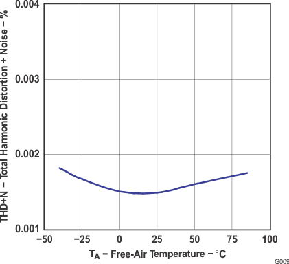 Figure 1. Total Harmonic Distortion + Noise
 vs Free-Air Temperature
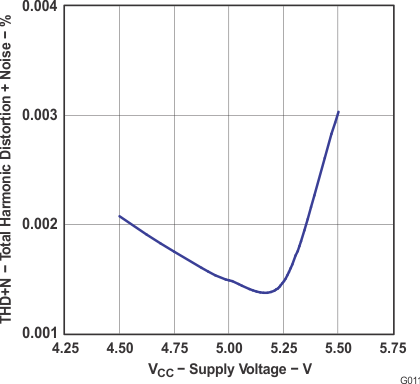 Figure 3. Total Harmonic Distortion + Noise
 vs Supply Voltage
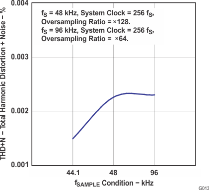 Figure 5. Total Harmonic Distortion + Noise
 vs fSAMPLE Condition
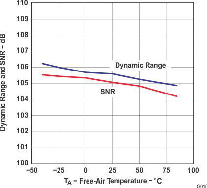 Figure 2. Dynamic Range and SNR
vs Free-Air Temperature
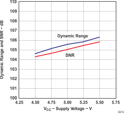 Figure 4. Dynamic Range and SNR vs Suppy Voltage
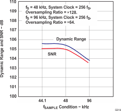 Figure 6. Dynamic Range and SNR vs fSAMPLE Condition
6.6.1 Typical Characteristics: Internal Filter
6.6.1.1 Digital Filter: Decimation Filter Frequency Response
TA = 25°C, VCC = 5 V, VDD = 3.3 V, Master mode, fS = 44.1 kHz, system clock = 384 fS, oversampling ratio = ×128, and 24-bit data (unless otherwise noted).
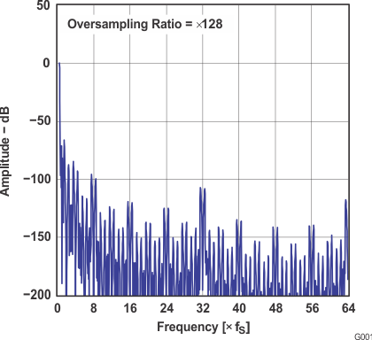 Figure 7. Amplitude vs Frequency Overall Characteristics
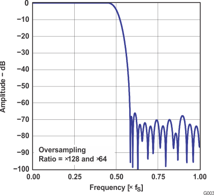 Figure 9. Amplitude vs Frequency Stop-Band Attenuation Characteristics
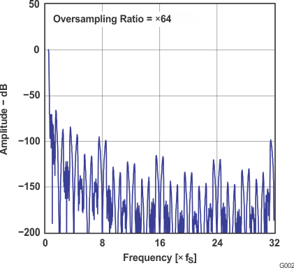 Figure 8. Amplitude vs Frequency Overall Characteristics
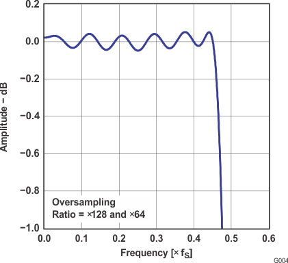 Figure 10. Amplitude vs Frequency Pass-Band Ripple Characteristics
6.6.1.2 HPF (High-Pass Filter) Frequency Response
TA = 25°C, VCC = 5 V, VDD = 3.3 V, Master mode, fS = 44.1 kHz, system clock = 384 fS, oversampling ratio = ×128, and 24-bit data (unless otherwise noted).
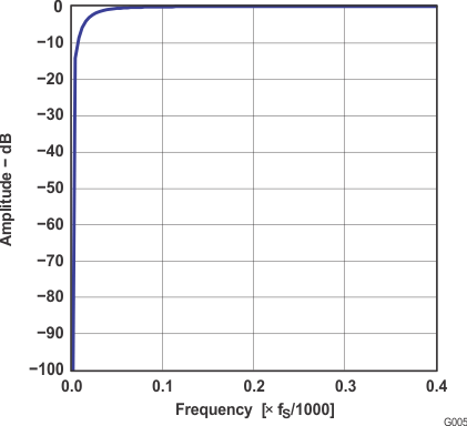 Figure 11. Amplitude vs Frequency HPF
Stop-Band Characteristics
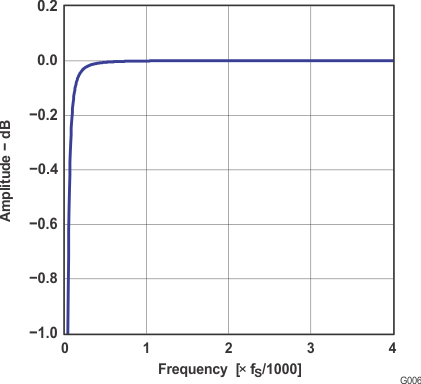 Figure 12. Amplitude vs Frequency HPF
Pass-Band Characteristics
6.6.1.3 Analog Filter: Antialiasing Filter Frequence Response
TA = 25°C, VCC = 5 V, VDD = 3.3 V, Master mode, fS = 44.1 kHz, system clock = 384 fS, oversampling ratio = ×128, and 24-bit data (unless otherwise noted).
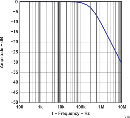 Figure 13. Amplitude vs Frequency Antialias Filter Stop-Band Characteristics
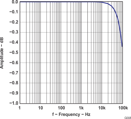 Figure 14. Amplitude vs Frequency Antialias Filter Pass-Band Characteristics
6.6.2 Typical Characteristics: Output Spectrum
TA = 25°C, VCC = 5 V, VDD = 3.3 V, Master mode, fS = 44.1 kHz, system clock = 384 fS, oversampling ratio = ×128, and 24-bit data (unless otherwise noted).
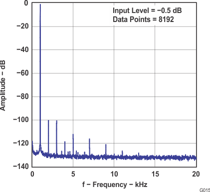 Figure 15. Amplitude vs Frequency
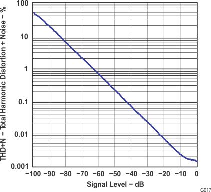 Figure 17. Total Harmonic Distortion + Noise vs Signal Level
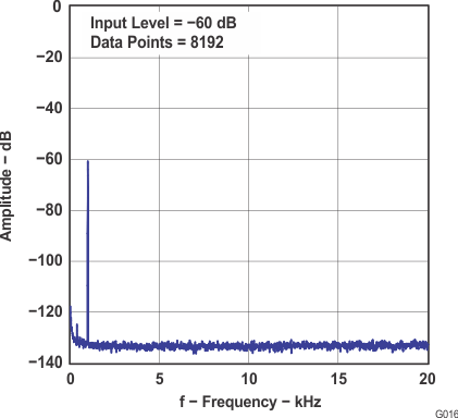 Figure 16. Amplitude vs Frequency
6.6.3 Typical Characteristics: Supply Current
TA = 25°C, VCC = 5 V, VDD = 3.3 V, Master mode, fS = 44.1 kHz, system clock = 384 fS, oversampling ratio = ×128, and 24-bit data (unless otherwise noted).
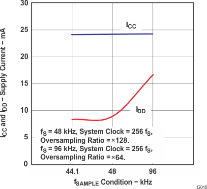 Figure 18. Supply Current vs fSAMPLE Condition