SLAS859C May 2012 – May 2015 PCM5100A , PCM5100A-Q1 , PCM5101A , PCM5101A-Q1 , PCM5102A , PCM5102A-Q1
PRODUCTION DATA.
- 1 Features
- 2 Applications
- 3 Description
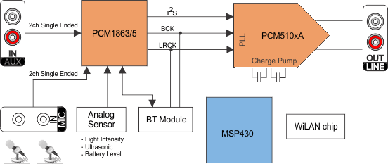
- 4 Simplified System Diagram
- 5 Revision History
- 6 Device Comparison
- 7 Pin Configuration and Functions
- 8 Specifications
- 9 Detailed Description
- 10Applications and Implementation
- 11Power Supply Recommendations
- 12Layout
- 13Device and Documentation Support
- 14Mechanical, Packaging, and Orderable Information
1 Features
- Ultra Low Out-of-Band Noise
- Integrated High-Performance Audio PLL with BCK Reference to Generate SCK Internally
- Direct Line Level 2.1-VRMS Output
- No DC Blocking Capacitors Required
- Line Level Output Down to 1KΩ
- Intelligent Muting System; Soft Up or Down Ramp and Analog Mute For 120-dB Mute SNR
- Accepts 16-, 24-, and 32-Bit Audio Data
- PCM Data Formats: I2S, Left-Justified
- Automatic Power-Save Mode When LRCK And BCK Are Deactivated
- 1.8 V or 3.3 V Failsafe LVCMOS Digital Inputs
- Simple Configuration Using Hardware Pins
- Single-Supply Operation: 14
- 3.3 V Analog, 1.8 V or 3.3 V Digital
- Qualified in Accordance with AEC-Q100
2 Applications
- A/V Receivers, DVD, BD Players
- Automotive Infotainment and Telematics
- HDTV Receivers
- Aftermarket Automotive Amplifiers
3 Description
The PCM510xA devices are a family of monolithic CMOS-integrated circuits that include a stereo digital-to-analog converter and additional support circuitry in a small TSSOP package. The PCM510xA devices use the latest generation of TI’s advanced segment-DAC architecture to achieve excellent dynamic performance and improved tolerance to clock jitter.
Using Directpath™ charge-pump technology, the PCM510xA devices provide 2.1-VRMS ground centered outputs, allowing designers to eliminate DC blocking capacitors on the output, as well as external muting circuits traditionally associated with single-supply line drivers.
The integrated line driver surpasses all other charge-pump based line drivers by supporting loads down to 1 kΩ per pin.
The integrated PLL on the device removes the requirement for a system clock (commonly known as master clock), allowing a 3-wire I2S connection and reducing system EMI.
Intelligent clock error and PowerSense undervoltage protection utilizes a two-level mute system for pop-free performance.
Compared with many conventional switched capacitor DAC architectures, the PCM510xA family offers up to 20 dB lower out-of-band noise, reducing EMI and aliasing in downstream amplifiers/ADCs, measured from the traditional 100-kHz OBN measurements to 3 MHz).
Table 1. Device Information(1)
| PART NUMBER | PACKAGE | BODY SIZE (NOM) |
|---|---|---|
| PCM5102A | TSSOP (20) | 5.50 mm × 4.40 mm |
| PCM5101A | ||
| PCM5100A |
- For all available packages, see the orderable addendum at the end of the data sheet.
