SLAS859C May 2012 – May 2015 PCM5100A , PCM5100A-Q1 , PCM5101A , PCM5101A-Q1 , PCM5102A , PCM5102A-Q1
PRODUCTION DATA.
- 1 Features
- 2 Applications
- 3 Description
- 4 Simplified System Diagram
- 5 Revision History
- 6 Device Comparison
- 7 Pin Configuration and Functions
- 8 Specifications
- 9 Detailed Description
- 10Applications and Implementation
- 11Power Supply Recommendations
- 12Layout
- 13Device and Documentation Support
- 14Mechanical, Packaging, and Orderable Information
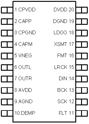
7 Pin Configuration and Functions
PW 20-Pin Package
(Top View)

Pin Functions
| PIN | TYPE | DESCRIPTION | |
|---|---|---|---|
| NAME | NO. | ||
| AGND | 9 | — | Analog ground |
| AVDD | 8 | P | Analog power supply, 3.3 V |
| BCK | 13 | I | Audio data bit clock input(1) |
| CAPM | 4 | O | Charge pump flying capacitor terminal for negative rail |
| CAPP | 2 | O | Charge pump flying capacitor terminal for positive rail |
| CPGND | 3 | — | Charge pump ground |
| CPVDD | 1 | P | Charge pump power supply, 3.3 V |
| DEMP | 10 | I | De-emphasis control for 44.1-kHz sampling rate(1): Off (Low) / On (High) |
| DGND | 19 | — | Digital ground |
| DIN | 14 | I | Audio data input(1) |
| DVDD | 20 | P | Digital power supply, 1.8 V or 3.3 V |
| FLT | 11 | I | Filter select : Normal latency (Low) / Low latency (High) |
| FMT | 16 | I | Audio format selection : I2S (Low) / Left-justified (High) |
| LDOO | 18 | P | Internal logic supply rail terminal for decoupling, or external 1.8 V supply terminal |
| LRCK | 15 | I | Audio data word clock input(1) |
| OUTL | 6 | O | Analog output from DAC left channel |
| OUTR | 7 | O | Analog output from DAC right channel |
| SCK | 12 | I | System clock input(1) |
| VNEG | 5 | O | Negative charge pump rail terminal for decoupling, –3.3 V |
| XSMT | 17 | I | Soft mute control(1): Soft mute (Low) / soft un-mute (High) |
(1) Failsafe LVCMOS Schmitt trigger input