JAJSIV0B June 2009 – March 2020 PGA280
PRODUCTION DATA.
- 1 特長
- 2 アプリケーション
- 3 概要
- 4 改訂履歴
- 5 概要(続き)
- 6 Pin Configuration and Functions
- 7 Specifications
-
8 Detailed Description
- 8.1 Overview
- 8.2 Functional Block Diagram
- 8.3 Feature Description
- 8.4 Device Functional Modes
- 8.5 Programming
- 8.6
Register Map
- 8.6.1 Register 0: Gain and External MUX Address (address = 00h) [reset = 0000 0000b]
- 8.6.2 Register 1: Software Reset Register (address = 01h) [reset = 0000 0000b]
- 8.6.3 Register 2: SPI: MODE Selection to GPIO-Pin (address = 02h) [reset = 0000 0000b]
- 8.6.4 Register 3: BUF Timeout Register (address = 03h) [reset = 0001 1001b]
- 8.6.5 Register 4: Error Register (address = 04h) [reset = 0000 0000b]
- 8.6.6 Register 5: GPIO Register (address = 05h) [reset = 0000 0000b]
- 8.6.7 Register 6: Input Switch Control Register 1 (address = 06h) [reset = 0110 0000b]
- 8.6.8 Register 7: Input Switch Control Register 2 (address =07h ) [reset = 0000 0000b]
- 8.6.9 Register 8: GPIO Configuration Register (address = 08h) [reset = 0000 0000b]
- 8.6.10 Register 9: CS Configuration Mode Register (address = 09h) [reset = 0000 0000b]
- 8.6.11 Register 10: Configuration Register 1 (address = 0Ah) [reset = 0000 0000b]
- 8.6.12 Register 11: Configuration Register 2 (address = 0Bh) [reset = 0001 0000b]
- 8.6.13 Register 12: Special Functions Register (address = 0Ch) [reset = 0000 0000b]
- 9 Application and Implementation
- 10Power Supply Recommendations
- 11デバイスおよびドキュメントのサポート
- 12メカニカル、パッケージ、および注文情報
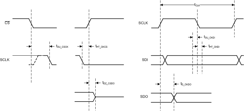
7.3 Timing Requirements: Serial Interface
at TA = –40°C to +105°C, DVDD = 2.7 V to 5.5 V, and CLOAD on SDO = 20 pF (unless otherwise specified)| MIN | NOM | MAX | UNIT | ||
|---|---|---|---|---|---|
| fSCLK | Serial clock frequency | 16 | MHz | ||
| tCLK | Serial clock time period | 62.5 | ns | ||
| tSU_CSCK | Setup time: CS falling to first SCLK capture (falling) edge | 0 | ns | ||
| tHT_CKCS | Delay time: last SCK capture (falling) to CS rising | 0 | ns | ||
| tSU_CKDI | Setup time: SDI data valid to SCLK capture (falling) edge | 5 | ns | ||
| tHT_CKDI | Hold time: SCLK capture (falling) edge to previous data valid on SDI | 10 | ns | ||
| tDZ_CSDO | Delay time: CS rising to SDO going to Hi-Z | 25 | ns | ||
| tD_CKDO | Delay time: SCLK rising edge to (next) data valid on SDO | 25 | ns | ||
 Figure 1. Serial Timing Diagram