JAJSIV0B June 2009 – March 2020 PGA280
PRODUCTION DATA.
- 1 特長
- 2 アプリケーション
- 3 概要
- 4 改訂履歴
- 5 概要(続き)
- 6 Pin Configuration and Functions
- 7 Specifications
-
8 Detailed Description
- 8.1 Overview
- 8.2 Functional Block Diagram
- 8.3 Feature Description
- 8.4 Device Functional Modes
- 8.5 Programming
- 8.6
Register Map
- 8.6.1 Register 0: Gain and External MUX Address (address = 00h) [reset = 0000 0000b]
- 8.6.2 Register 1: Software Reset Register (address = 01h) [reset = 0000 0000b]
- 8.6.3 Register 2: SPI: MODE Selection to GPIO-Pin (address = 02h) [reset = 0000 0000b]
- 8.6.4 Register 3: BUF Timeout Register (address = 03h) [reset = 0001 1001b]
- 8.6.5 Register 4: Error Register (address = 04h) [reset = 0000 0000b]
- 8.6.6 Register 5: GPIO Register (address = 05h) [reset = 0000 0000b]
- 8.6.7 Register 6: Input Switch Control Register 1 (address = 06h) [reset = 0110 0000b]
- 8.6.8 Register 7: Input Switch Control Register 2 (address =07h ) [reset = 0000 0000b]
- 8.6.9 Register 8: GPIO Configuration Register (address = 08h) [reset = 0000 0000b]
- 8.6.10 Register 9: CS Configuration Mode Register (address = 09h) [reset = 0000 0000b]
- 8.6.11 Register 10: Configuration Register 1 (address = 0Ah) [reset = 0000 0000b]
- 8.6.12 Register 11: Configuration Register 2 (address = 0Bh) [reset = 0001 0000b]
- 8.6.13 Register 12: Special Functions Register (address = 0Ch) [reset = 0000 0000b]
- 9 Application and Implementation
- 10Power Supply Recommendations
- 11デバイスおよびドキュメントのサポート
- 12メカニカル、パッケージ、および注文情報
8.5.4 Buffer Timing
The buffer is used to isolate fast transients from the overload protection of the high-precision amplifier. The buffer avoids current into the overload clamp. Fast transients result from the switching transient of a signal multiplexer or a gain change; these transients cannot be filtered in the signal path.
The buffer can be turned on by software using the T bit in the SPI command or by activating a GPIO pin. The on-time of the buffer is set in Register 3 (BUFTIM).
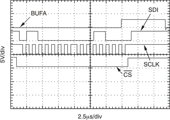
If controlled by software command, the buffer turns active (indicated by BUFA shown in Figure 55) with the last falling edge of SCLK.
Controlling an external MUX through Register 0 activates the GPIO pins after the rising edge of CS, providing an extra delay.
Alternatively, the buffer can be controlled by GPIO4, after configuration (Register 8, bit 4 = 0, and 0x4C10). A rising edge triggers the buffer with a delay of three to four clock cycles. If held high, the buffer [BUFA] remains active. The active time is extended by a minimum of three to four clock cycles plus FLAGTIM.
The buffer active condition can be observed at GPIO5, after configuration for output and special function (0x4820, 0x4C20). The time reference is the end of CS. The buffer is turned on with the 16th falling edge of the SCLK and writing to Register 0 (0x6018). BUFA stays high for 6 μs (BUFTIM0) after CS.
 Figure 55. BUFA Timing