JAJSPR4B April 2023 – September 2023 PGA855
PRODUCTION DATA
- 1
- 1 特長
- 2 アプリケーション
- 3 概要
- 4 Revision History
- 5 Device Comparison Table
- 6 Pin Configuration and Functions
- 7 Specifications
- 8 Detailed Description
- 9 Application and Implementation
- 10Device and Documentation Support
- 11Mechanical, Packaging, and Orderable Information
パッケージ・オプション
メカニカル・データ(パッケージ|ピン)
- RGT|16
サーマルパッド・メカニカル・データ
- RGT|16
発注情報
7.6 Typical Characteristics
at TA = 25°C, VS = VSOUT = ±15 V, VICM = VOCM = 0 V, RL = 10 kΩ, and G = 1 V/V (unless otherwise noted)
Table 7-1 Table of Graphs
| DESCRIPTION | FIGURE |
|---|---|
| Distribution of Offset Voltage (RTI), G = 16 V/V | Figure 7-1 |
| Distribution of Offset Voltage Drift (RTI), G = 16 V/V | Figure 7-2 |
| Distribution of Offset Voltage (RTI), G = 1 V/V | Figure 7-3 |
| Distribution of Offset Voltage Drift (RTI), G = 1 V/V | Figure 7-4 |
| Distribution of Offset Voltage (RTI), G = 0.125 V/V | Figure 7-5 |
| Distribution of Offset Voltage Drift (RTI), G = 0.125 V/V | Figure 7-6 |
| Distribution of Differential Gain Error, G = 16 V/V | Figure 7-7 |
| Distribution of Differential Gain Error, G = 1 V/V | Figure 7-8 |
| Gain Error vs Temperature, G = 1 V/V | Figure 7-9 |
| Distribution of Differential Gain Error, G = 0.125 V/V | Figure 7-10 |
| Distribution of Input Bias Current | Figure 7-11 |
| Distribution of Input Bias Current, TA = 85°C | Figure 7-12 |
| Input Bias Current vs Temperature | Figure 7-13 |
| Input Bias Current vs Input Common-Mode Voltage | Figure 7-14 |
| Distribution of Input Offset Current | Figure 7-15 |
| Input Offset Current vs Temperature | Figure 7-16 |
| Offset Voltage (RTI) vs Temperature, G = 16 V/V | Figure 7-17 |
| Offset Voltage (RTI) vs Temperature | Figure 7-18 |
| Offset Voltage (RTI) vs Temperature, G = 0.125 V/V | Figure 7-19 |
| Offset Voltage (RTI) vs Input Common-Mode Voltage | Figure 7-20 |
| CMRR Distribution, G = 16 V/V | Figure 7-21 |
| CMRR Distribution, G = 1 V/V | Figure 7-22 |
| CMRR Distribution, G = 0.125V/V | Figure 7-23 |
| CMRR vs Frequency (RTI) | Figure 7-24 |
| CMRR vs Frequency (Unbalanced) | Figure 7-25 |
| Typical CMRR vs Temperature | Figure 7-26 |
| Positive PSRR vs Frequency | Figure 7-27 |
| Negative PSRR vs Frequency | Figure 7-28 |
| PSRR Distribution, G = 16 V/V | Figure 7-29 |
| PSRR Distribution, G = 1 V/V | Figure 7-30 |
| PSRR Distribution, G = 0.125 V/V | Figure 7-31 |
| Gain Nonlinearity, G = 16 V/V | Figure 7-32 |
| Gain Nonlinearity, G = 1 V/V | Figure 7-33 |
| Gain Nonlinearity, G = 0.125 V/V | Figure 7-34 |
| Voltage Noise Spectral Density (RTI) vs Frequency | Figure 7-35 |
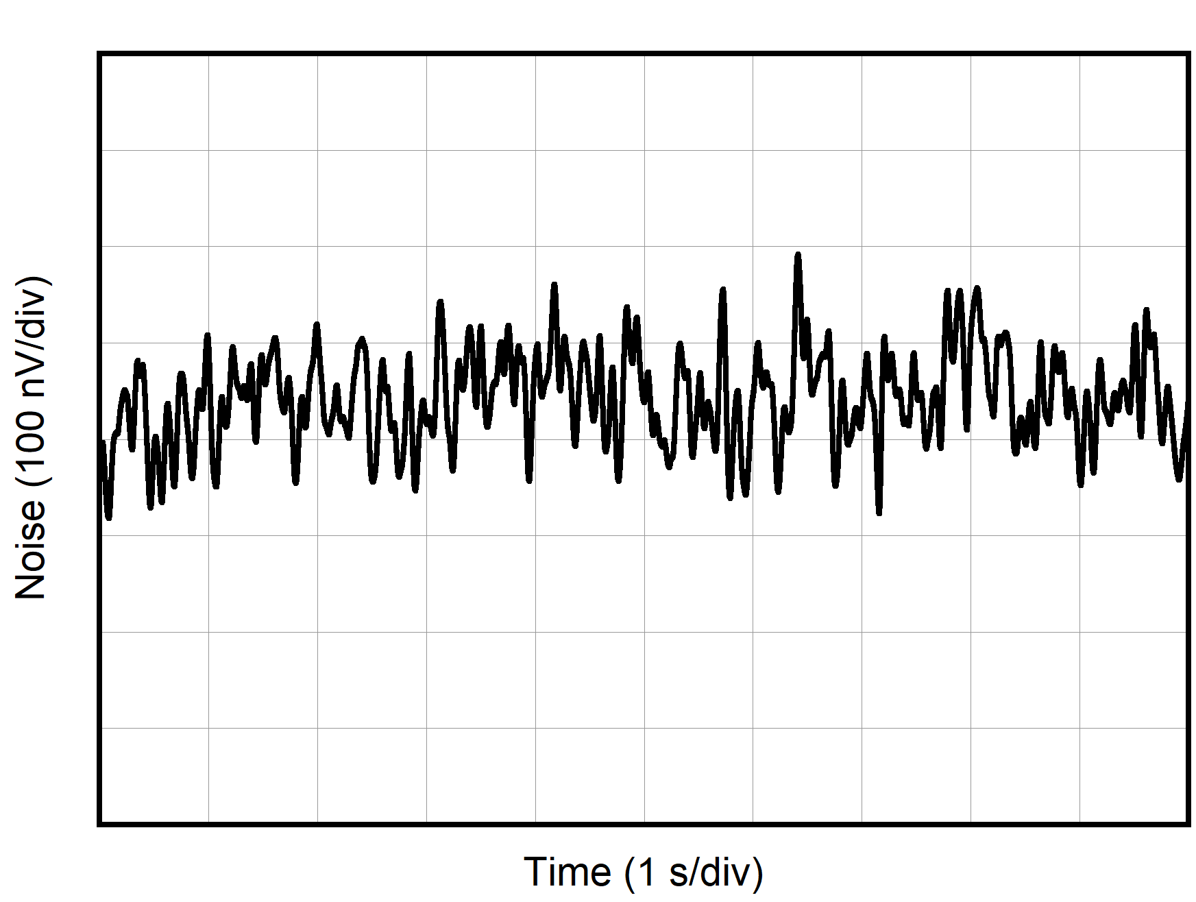
| 0.1-Hz to 10-Hz Voltage Noise (RTI), G = 16 V/V | Figure 7-36 |
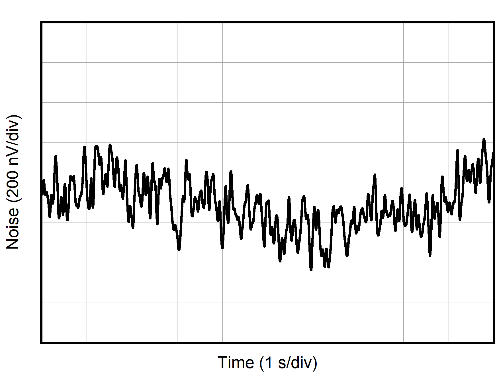
| 0.1-Hz to 10-Hz Voltage Noise (RTI), G = 1 V/V | Figure 7-37 |
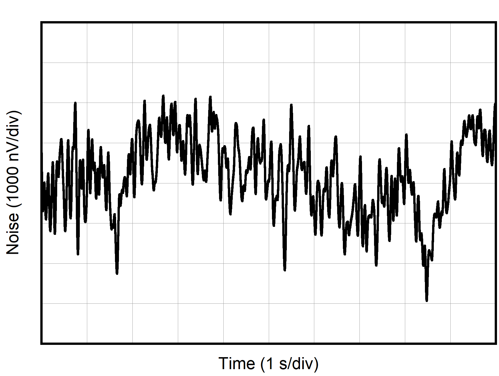
| 0.1-Hz to 10-Hz Voltage Noise (RTI), G = 0.125 V/V | Figure 7-38 |
| Current Noise Spectral Density vs Frequency | Figure 7-39 |
| Gain vs Frequency | Figure 7-40 |
| Large-Signal Step Response vs Frequency | Figure 7-41 |
| Small-Signal Step Response, G = 16 V/V | Figure 7-42 |
| Small-Signal Step Response, G = 1 V/V | Figure 7-43 |
| Small-Signal Step Response, G = 0.125 V/V | Figure 7-44 |
| Large-Signal Step Response | Figure 7-45 |
| Gain Switching Transient Response | Figure 7-46 |
| Output Short-Circuit Current vs Temperature | Figure 7-47 |
| Positive Output Voltage Swing vs Output Current | Figure 7-48 |
| Negative Output Voltage Swing vs Output Current | Figure 7-49 |
| Overload Recovery | Figure 7-50 |
| Closed-Loop Output Impedance vs Frequency | Figure 7-51 |
| Overshoot vs Capacitive Load | Figure 7-52 |
| Quiescent Current vs Temperature | Figure 7-53 |
| THD + Noise vs Frequency (22-kHz Filter) | Figure 7-54 |
| THD + Noise vs Frequency (500-kHz Filter) | Figure 7-55 |
| 2nd Harmonic Distortion vs Frequency | Figure 7-56 |
| 3rd Harmonic Distortion vs Frequency | Figure 7-57 |
| Total Harmonic Distortion vs Frequency vs Output Load | Figure 7-58 |
| Ax Digital Input Pin Current vs Ax Digital Input Pin Voltage | Figure 7-59 |
| DGND Digital Input Pin Current vs A2 Digital Input Pin Voltage | Figure 7-60 |
| Digital Input Pin Current vs Temperature | Figure 7-61 |

| N = 2500 | Mean = –21.25 µV | Std. dev. = 36.79 µV |
| G = 16 V/V | ||

| N = 2500 | Mean = 2.83 µV | Std. dev. = 71.58 µV |
| G = 1 V/V | ||

| N = 2500 | Mean = –36 µV | Std. dev. = 540 µV |
| G = 0.125 V/V | ||

| N = 7295 | Mean = 0.0257 % | Std. dev. = 0.0136 % |
| G = 16 V/V |


| N = 59 | Mean = –0.37 nA | Std. dev. = 0.183 nA |

| 59 units, 1 wafer lot |

| N = 59 | Mean = –0.007 nA | Std. dev. = 0.142 nA |

| G = 16 V/V | 53 units, 1 wafer lot |

| G = 0.125 V/V | 53 units, 1 wafer lot |

| N = 2500 | Mean = 0.31 µV/V | Std. dev. = 0.78 µV/V |
| G = 16 V/V | ||

| N = 2500 | Mean = 44.98 µV/V | Std. dev. = 100 µV/V |
| G = 0.125 V/V | ||


| Typical unit shown |

| N = 2500 | Mean = 0.13 µV/V | Std. dev. = 0.06 µV/V |
| G = 16 V/V | ||

| N = 2500 | Mean = 0.38 µV/V | Std. dev. = 0.48 µV/V |
| G = 0.125 V/V | ||

| G = 1 V/V | VOUTDIFF = 10 V |

| Typical unit shown |

| G = 1 V/V |

| G = 16 V/V |

| Differential load capacitance = 50 pF | ||

| G = 1 V/V | Differential load capacitance = 50 pF | |

| G = 1 V/V |

| Short to VSOUT/2 |

| VS = ±18 V | VSOUT = ±15 V | G = 16 V/V |


| 10-Hz to 500-kHz band-pass filter | VOUTDIFF > 2.5 VPP |

| VOUTDIFF > 2.5 VPP |

| DGND = –18 V |


| N = 53 | Mean = –0.11 µV/°C | Std. dev. = 0.08 µV/°C |
| G = 16 V/V | ||

| N = 53 | Mean = –0.024 µV/°C | Std. dev. = 0.22 µV/°C |
| G = 1 V/V | ||

| N = 53 | Mean = –0.028 µV/°C | Std. dev. = 1.69 µV/°C |
| G = 0.125 V/V | ||

| N = 7295 | Mean = 0.0195 % | Std. dev. = 0.0012 % |
| G = 1 V/V |

| N = 7295 | Mean = 0.0238% | Std. dev. = 0.008% |
| G = 0.125 V/V | ||

| N = 59 | Mean = –0.34 nA | Std. dev. = 0.16 nA |
| TA = 85°C |


| 59 units, 1 wafer lot |

| G = 1 V/V | 53 units, 1 wafer lot |

| Typical unit shown |

| N = 2500 | Mean = 5.61 µV/V | Std. dev. = 12.50 µV/V |
| G = 1 V/V | ||


| Typical unit shown |

| Typical unit shown |

| N = 2500 | Mean = 0.17 µV/V | Std. dev. = 0.08 µV/V |
| G = 1 V/V | ||

| G = 16 V/V | VOUTDIFF = 10 V | |

| G = 0.125 V/V | VOUTDIFF = 2.5 V |

| G = 16 V/V |

| G = 0.125 V/V |

| Differential load capacitance = 50 pF | ||

| G = 16 V/V | Differential load capacitance = 50 pF | |

| G = 0.125 V/V | Differential load capacitance = 50 pF | |

| Input voltage = 250 mVPP |

| VS = ±18 V | VSOUT = ±15 V | G = 16 V/V |


| 10-Hz to 22-kHz band-pass filter | VOUTDIFF > 2.5 VPP |

| VOUTDIFF > 2.5 VPP |

| G = 1 V/V | VOUTDIFF = 10 VPP |

| Ax = DGND |