JAJSDR2F September   2017  – June 2021 REF3425 , REF3430 , REF3433 , REF3440 , REF3450

PRODUCTION DATA  

  1. 特長
  2. アプリケーション
  3. 概要
  4. Revision History
  5. Device Comparison Table
  6. Pin Configuration and Functions
  7. Specifications
    1. 7.1 Absolute Maximum Ratings
    2. 7.2 ESD Ratings
    3. 7.3 Recommended Operating Conditions
    4. 7.4 Thermal Information
    5. 7.5 Electrical Characteristics
    6. 7.6 Typical Characteristics
  8. Parameter Measurement Information
    1. 8.1 Solder Heat Shift
    2. 8.2 Long-Term Stability
    3. 8.3 Thermal Hysteresis
    4. 8.4 Power Dissipation
    5. 8.5 Noise Performance
  9. Detailed Description
    1. 9.1 Overview
    2. 9.2 Functional Block Diagram
    3. 9.3 Feature Description
      1. 9.3.1 Supply Voltage
      2. 9.3.2 Low Temperature Drift
      3. 9.3.3 Load Current
    4. 9.4 Device Functional Modes
      1. 9.4.1 EN Pin
      2. 9.4.2 Negative Reference Voltage
  10. 10Application and Implementation
    1. 10.1 Application Information
    2. 10.2 Typical Application: Basic Voltage Reference Connection
      1. 10.2.1 Design Requirements
      2. 10.2.2 Detailed Design Procedure
        1. 10.2.2.1 Input and Output Capacitors
        2. 10.2.2.2 4-Wire Kelvin Connections
        3. 10.2.2.3 VIN Slew Rate Considerations
        4. 10.2.2.4 Shutdown/Enable Feature
      3. 10.2.3 Application Curves
  11. 11Power Supply Recommendations
  12. 12Layout
    1. 12.1 Layout Guidelines
    2. 12.2 Layout Example
  13. 13Device and Documentation Support
    1. 13.1 Documentation Support
      1. 13.1.1 Related Documentation
    2. 13.2 Receiving Notification of Documentation Updates
    3. 13.3 サポート・リソース
    4. 13.4 Trademarks
    5. 13.5 Electrostatic Discharge Caution
    6. 13.6 Glossary
  14. 14Mechanical, Packaging, and Orderable Information

パッケージ・オプション

メカニカル・データ(パッケージ|ピン)
サーマルパッド・メカニカル・データ
発注情報

Typical Characteristics

at TA = 25°C, VIN = VEN = 12 V, IL = 0 mA, CL = 10 µF, CIN = 0.1 µF (unless otherwise noted)

GUID-1CD69C0E-D3A9-4303-B1C8-FDF2DF9A7138-low.gifFigure 7-1 Temperature Drift
GUID-327B3618-B82B-4324-9911-F3961CB60002-low.gifFigure 7-3 Output Voltage Accuracy vs Temperature
GUID-EA2903BE-4142-436A-8BA7-71052E87405C-low.gifFigure 7-5 Power-Supply Rejection Ratio vs Frequency
GUID-7A1ADF6F-4CA7-48E5-99A8-CDBA1A8678F2-low.gifFigure 7-7 Load Regulation Sourcing
GUID-F7484669-5737-4712-851E-C64015357363-low.pngFigure 7-9 Noise Performance 10 Hz to 10 kHz
GUID-4D2FDB08-6117-4F2D-8757-9DA70D84159B-low.gifFigure 7-11 Load Transient
GUID-2A8E2047-3F12-41F4-A841-D7C4FDA921A6-low.gifFigure 7-13 Load Transient
GUID-5F82D5DD-63F1-4BA4-B682-B2960C3707EB-low.gifFigure 7-15 Line Transient
GUID-98196DCE-CE9C-4726-9CE9-CB4F47A0E85C-low.gifFigure 7-17 Thermal Hysteresis Distribution (Cycle 1)
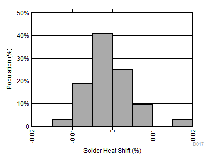
GUID-AE69A098-61D6-4054-B7D8-54B38733D1BF-low.gif
Refer to Section 8.1 for more information
Figure 7-19 Solder Heat Shift Distribution
GUID-FBF72FD4-8F91-42DB-8C3F-5937D5C29675-low.gifFigure 7-21 0.1-Hz to 10-Hz Noise (VOUT)
GUID-ABD1191E-A1E5-4EC4-B0A2-7BFF306F7732-low.gif
 
Figure 7-2 VIN vs IQ over Temperature
GUID-DCDF45AF-AA3A-4D1C-A477-CF7A887489E2-low.gifFigure 7-4 Quiescent Current vs Temperature
GUID-3962F902-29E8-4AEF-B318-54AFA851DC8A-low.gifFigure 7-6 Line Regulation
GUID-588E585C-7591-4668-A4CB-F27FAC888442-low.gifFigure 7-8 Load Regulation Sinking
GUID-497C6590-9805-4A1B-9190-C7A87BA0C2B5-low.gif
 
Figure 7-10 Load Transient
GUID-B7AD0287-C8FC-4372-BB5D-90EB438DED65-low.gifFigure 7-12 Load Transient
GUID-CB251955-EE2E-4713-8E43-776E22E47005-low.gifFigure 7-14 Line Transient
GUID-876C39EF-8392-4EBF-B41F-B36AD55D334F-low.gifFigure 7-16 Quiescent Current Shutdown Mode
GUID-D8635073-378E-4EBC-B691-D72930666755-low.gifFigure 7-18 Thermal Hysteresis Distribution (Cycle 2)
GUID-04145224-63E9-446E-A2CC-FA2BB5736AEE-low.gif
 
 
Figure 7-20 Turnon Time (Enable)
GUID-E0EBA014-3DD8-490E-972A-F2C312338495-low.gifFigure 7-22 Long Term Stability - 1000 hours (VOUT)