JAJSL60F April   1977  – January 2021 SG2524 , SG3524

PRODUCTION DATA  

  1. 特長
  2. アプリケーション
  3. 概要
  4. Revision History
  5. Pin Configurations and Functions
    1.     Pin Functions
  6. Specifications
    1. 6.1 Absolute Maximum Ratings
    2. 6.2 ESD Ratings
    3. 6.3 Recommended Operating Conditions
    4. 6.4 Thermal Information
  7. 12
    1. 7.1 Electrical Characteristics
    2. 7.2 Electrical Characteristics — Continued, Both Parts
    3. 7.3 Typical Characteristics
  8. Parameter Measurement Information
    1. 8.1 17
  9. Detailed Description
    1. 9.1 Overview
    2. 9.2 Functional Block Diagram
    3. 9.3 Feature Description
      1. 9.3.1 Blanking
      2. 9.3.2 Error Amplifier
      3. 9.3.3 Compensation
      4. 9.3.4 Output Circuitry
      5. 9.3.5 Current Limiting
    4. 9.4 Device Functional Modes
      1. 9.4.1 Synchronous Operation
      2. 9.4.2 Shutdown Circuitry
        1.       Application and Implementation
          1. 10.1 Application Information
          2. 10.2 Typical Application
            1. 10.2.1 Capacitor-Diode Output
              1. 10.2.1.1 Design Requirements
              2. 10.2.1.2 Detailed Design Procedure
                1. 10.2.1.2.1 Oscillator
                2. 10.2.1.2.2 Voltage Reference
              3. 10.2.1.3 Application Curves
          3. 10.3 Examples of Other Output Stages
            1. 10.3.1 Flyback Converter
            2. 10.3.2 Single-Ended LC
            3. 10.3.3 Push-Pull Transformer-Coupled
              1.          Power Supply Recommendations
  10. 10Layout
    1. 10.1 Layout Guidelines
      1. 10.1.1 Feedback Traces
      2. 10.1.2 Input/Output Capacitors
      3. 10.1.3 Compensation Components
      4. 10.1.4 Traces and Ground Planes
    2. 10.2 Layout Example
  11. 11Device and Documentation Support
    1. 11.1 Related Links
    2. 11.2 Trademarks
      1.      Mechanical, Packaging, and Orderable Information

パッケージ・オプション

デバイスごとのパッケージ図は、PDF版データシートをご参照ください。

メカニカル・データ(パッケージ|ピン)
  • N|16
  • D|16
サーマルパッド・メカニカル・データ
発注情報

Application Information

There are a wide variety of output configurations possible when considering the application of the SG2524 as a voltage-regulator control circuit. They can be segregated into three basic categories:

  • Capacitor-diode-coupled voltage multipliers
  • Inductor-capacitor-implemented single-ended circuits
  • Transformer-coupled circuits

Examples of these categories are shown in Figure 10-1, Figure 10-2, and Figure 10-3, respectively. Section 10.2 demonstrates how to set up the SG2524 for a capacitor-diode output design. The same techniques for setting up the internal circuitry of the IC may also be used for the other two output stage examples shown Section 10.3.
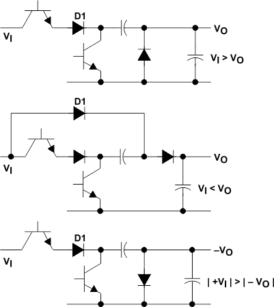
GUID-1E1067AF-19BD-4B3F-A0CE-57489EFCA54D-low.gifFigure 10-1 Capacitor-Diode-Coupled Voltage-Multiplier Output Stages
GUID-3D4C95D6-00CE-4478-8A45-B5A319A1C69B-low.gifFigure 10-2 Single-Ended Inductor Circuit
GUID-2B954BB9-F6E9-4DCE-9D7F-F644CB0B3A53-low.gifFigure 10-3 Transformer-Coupled Outputs