JAJSG48Q July 1995 – September 2018 SN54LVCH245A , SN74LVCH245A
PRODUCTION DATA.
- 1 特長
- 2 アプリケーション
- 3 概要
- 4 改訂履歴
- 5 Pin Configuration and Functions
-
6 Specifications
- 6.1 Absolute Maximum Ratings
- 6.2 ESD Ratings
- 6.3 Recommended Operating Conditions: SN74LVCH245A
- 6.4 Recommended Operating Conditions: SN54LVCH245A
- 6.5 Thermal Information
- 6.6 Electrical Characteristics: SN74LVCH245A
- 6.7 Electrical Characteristics: SN54LVCH245A
- 6.8 Switching Characteristics: SN74LVCH245A, –40°C TO 85°C
- 6.9 Switching Characteristics: SN74LVCH245A, –40°C TO 125°C
- 6.10 Switching Characteristics: SN54LVCH245A
- 6.11 Operating Characteristics
- 6.12 Typical Characteristics
- 7 Parameter Measurement Information
- 8 Detailed Description
- 9 Application and Implementation
- 10Power Supply Recommendations
- 11Layout
- 12デバイスおよびドキュメントのサポート
- 13メカニカル、パッケージ、および注文情報
パッケージ・オプション
デバイスごとのパッケージ図は、PDF版データシートをご参照ください。
メカニカル・データ(パッケージ|ピン)
- W|20
- J|20
- FK|20
サーマルパッド・メカニカル・データ
発注情報
7 Parameter Measurement Information

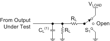
1. CL includes probe and jig capacitance.
Figure 3. Load Circuit Table 1. Test Load Switch Position
| TEST | S1 |
|---|---|
| tPLH / tPHL | Open |
| tPLZ / tPZL | VLOAD |
| tPHZ / tPZH | GND |
Table 2. Test and Measurement Conditions
| VCC | INPUTS | VM | VLOAD | CL | RL | VΔ | |
|---|---|---|---|---|---|---|---|
| VI | tr/tf | ||||||
| 1.8 V ± 0.15 V | VCC | ≤ 2 ns | VCC / 2 | 2 × VCC | 30 pF | 1 kΩ | 0.15 V |
| 2.5 V ± 0.2 V | VCC | ≤ 2 ns | VCC / 2 | 2 × VCC | 30 pF | 500 Ω | 0.15 V |
| 2.7 V | 2.7 V | ≤ 2.5 ns | 1.5 V | 6 V | 50 pF | 500 Ω | 0.3 V |
| 3.3 V ± 0.3 V | 2.7 V | ≤ 2.5 ns | 1.5 V | 6 V | 50 pF | 500 Ω | 0.3 V |

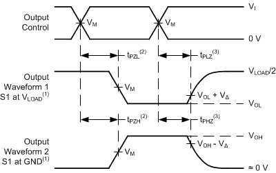
1. Waveform 1 is for an output with internal conditions such that the output is low, except when disabled by the output control.
Waveform 2 is for an output with internal conditions such that the output is high, except when disabled by the output control.
Waveform 2 is for an output with internal conditions such that the output is high, except when disabled by the output control.
2. tPZL and tPZH are the same as ten.
3. tPLZ and tPHZ are the same as tdis.
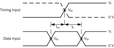
Figure 4. Voltage Waveforms Enable and Disable Times Low- and High-Level Enabling  Figure 6. Voltage Waveforms Setup and Hold Times
  Figure 5. Voltage Waveforms Pulse Duration
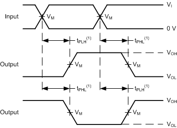
1. tPLH and tPHL are the same as tpd.
Figure 7. Voltage Waveforms Propagation Delay Times Inverting and Noninverting Outputs