JAJSK49C June 2013 – March 2021 SN6501-Q1
PRODUCTION DATA
- 1 特長
- 2 アプリケーション
- 3 説明
- 4 Revision History
- 5 Pin Configuration and Functions
- 6 Specifications
- 7 Parameter Measurement Information
- 8 Detailed Description
- 9 Application and Implementation
- 10Power Supply Recommendations
- 11Layout
- 12Device and Documentation Support
- 13Mechanical, Packaging, and Orderable Information
8.3.2 Core Magnetization
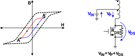
Figure 8-2 shows the ideal magnetizing curve for a push-pull converter with B as the magnetic flux density and H as the magnetic field strength. When Q1 conducts the magnetic flux is pushed from A to A’, and when Q2 conducts the flux is pulled back from A’ to A. The difference in flux and thus in flux density is proportional to the product of the primary voltage, VP, and the time, tON, it is applied to the primary: B ≈ VP × tON.
 Figure 8-2 Core Magnetization and Self-Regulation Through Positive Temperature Coefficient of RDS(on)
This volt-seconds (V-t) product is important as it determines the core magnetization during each switching cycle. If the V-t products of both phases are not identical, an imbalance in flux density swing results with an offset from the origin of the B-H curve. If balance is not restored, the offset increases with each following cycle and the transformer slowly creeps toward the saturation region.
Fortunately, due to the positive temperature coefficient of a MOSFET’s on-resistance, the output FETs of the SN6501 have a self-correcting effect on V-t imbalance. In the case of a slightly longer on-time, the prolonged current flow through a FET gradually heats the transistor which leads to an increase in RDS-on. The higher resistance then causes the drain-source voltage, VDS, to rise. Because the voltage at the primary is the difference between the constant input voltage, VIN, and the voltage drop across the MOSFET, VP = VIN – VDS, VP is gradually reduced and V-t balance restored.