JAJSPG7B April 1998 – January 2023 SN65ALS1176
PRODUCTION DATA
- 1 特長
- 2 アプリケーション
- 3 概要
- 4 Revision History
- 5 Pin Configuration and Functions
- 6 Specifications
- 7 Parameter Measurement Information
- 8 Detailed Description
- 9 Application and Implementation
- 10Device and Documentation Support
- 11Mechanical, Packaging, and Orderable Information
パッケージ・オプション
デバイスごとのパッケージ図は、PDF版データシートをご参照ください。
メカニカル・データ(パッケージ|ピン)
- D|8
サーマルパッド・メカニカル・データ
発注情報
7 Parameter Measurement Information
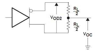 Figure 7-1 Driver VOD2 and
VOC Test Circuit
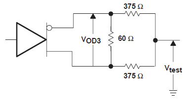 Figure 7-2 Driver VOD3 Test
Circuit
A. CL includes probe and jig capacitance.
B. The
input pulse is supplied by a generator having the following characteristics: PRR
≤ 1 MHz, 50% duty cycle, tr ≤ 6 ns, tf ≤ 6 ns,
ZO = 50 Ω.
C. td(OD) = td(ODH) or td(ODL).
Figure 7-3 Driver Differential-Output
Delay and Transition Times
A. CL includes probe and jig capacitance.
B. The
input pulse is supplied by a generator having the following characteristics: PRR
≤ 1 MHz, 50% duty cycle, tr ≤ 6 ns, tf ≤ 6 ns,
ZO = 50 Ω.
Figure 7-4 Driver Enable and Disable
Times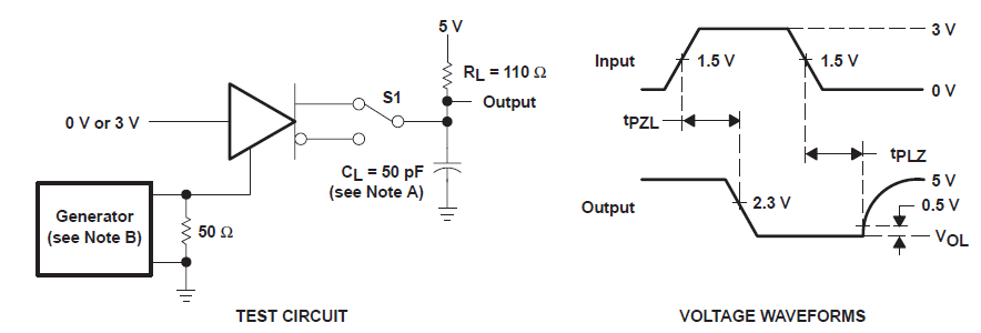
A. CL includes probe and jig capacitance.
B. The
input pulse is supplied by a generator having the following characteristics: PRR
≤ 1 MHz, 50% duty cycle, tr ≤ 6 ns, tf ≤ 6 ns,
ZO = 50 Ω.
Figure 7-5 Driver Enable and Disable
Times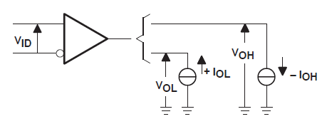 Figure 7-6 Receiver VOH and
VOL Test Circuit
A. CL includes probe and jig capacitance.
B. The
input pulse is supplied by a generator having the following characteristics: PRR
≤ 1 MHz, 50% duty cycle, tr ≤ 6 ns, tf ≤ 6 ns,
ZO = 50 Ω.
C. tpd = tPLH or tPHL.
Figure 7-7 Receiver Propagation-Delay
Times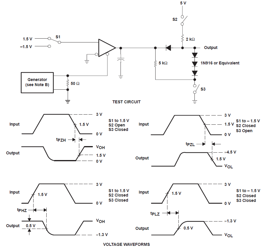
A. CL includes probe and jig capacitance.
B. The
input pulse is supplied by a generator having the following characteristics: PRR
≤ 1 MHz, 50% duty cycle, tr ≤ 6 ns, tf ≤ 6 ns,
ZO = 50 Ω.
Figure 7-8 Receiver Output Enable and
Disable Times