JAJSDL3D March 2016 – October 2024 SN65DPHY440SS , SN75DPHY440SS
PRODUCTION DATA
- 1
- 1 特長
- 2 アプリケーション
- 3 概要
- 4 Pin Configuration and Functions
- 5 Specifications
-
6 Detailed Description
- 6.1 Overview
- 6.2 Functional Block Diagram
- 6.3 Feature Description
- 6.4 Device Functional Modes
- 6.5
Register Maps
- 6.5.1 BIT Access Tag Conventions
- 6.5.2 Standard CSR Registers (address = 0x000 - 0x07)
- 6.5.3 Standard CSR Register (address = 0x08)
- 6.5.4 Standard CSR Register (address = 0x09)
- 6.5.5 Standard CSR Register (address = 0x0A)
- 6.5.6 Standard CSR Register (address = 0x0B)
- 6.5.7 Standard CSR Register (address = 0x0D)
- 6.5.8 Standard CSR Register (address = 0x0E)
- 6.5.9 Standard CSR Register (address = 0x10) [reset = 0xFF]
- 6.5.10 Standard CSR Register (address = 0x11) [reset = 0xFF]
- 7 Application and Implementation
- 8 Device and Documentation Support
- 9 Revision History
- 10Mechanical, Packaging, and Orderable Information
パッケージ・オプション
メカニカル・データ(パッケージ|ピン)
- RHR|28
サーマルパッド・メカニカル・データ
- RHR|28
発注情報
6.3.4 Dynamic De-skew
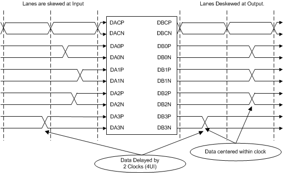
The DPHY440 implements a dynamic de-skew feature which will continuously de-skew the HS data received on the DA[3:0]P/N interface and provide a retimed version on the DB[3:0]P/N interface. The retimed version is centered within the DBCP/N clock.
 Figure 6-1 Dynamic De-skew
Note:
The dynamic de-skew feature is only enabled in HS mode, and causes a 2 clock (4 UI) delay of data while data traverses from DA to DB.