JAJSFO1G September 2012 – June 2018 SN65DSI84
PRODUCTION DATA.
- 1 特長
- 2 アプリケーション
- 3 概要
- 4 改訂履歴
- 5 Pin Configuration and Functions
- 6 Specifications
- 7 Detailed Description
- 8 Application and Implementation
- 9 Power Supply Recommendations
- 10Layout
- 11デバイスおよびドキュメントのサポート
- 12メカニカル、パッケージ、および注文情報
6.6 Switching Characteristics
over operating free-air temperature range (unless otherwise noted)| PARAMETER | TEST CONDITIONS | MIN | TYP(1) | MAX | UNIT | |
|---|---|---|---|---|---|---|
| DSI | ||||||
| tGS | DSI LP glitch suppression pulse width | 300 | ps | |||
| LVDS | ||||||
| tc | Output clock period | 6.49 | 40 | ns | ||
| tw | High-level output clock (CLK) pulse duration | 4/7 tc | ns | |||
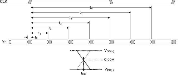
| t0 | Delay time, CLK↑ to 1st serial bit position | tc = 6.49ns;
Input clock jitter < 25ps (REFCLK) |
-0.15 | 0.15 | ns | |
| t1 | Delay time, CLK↑ to 2nd serial bit position | 1/7 tc – 0.15 | 1/7 tc + 0.15 | ns | ||
| t2 | Delay time, CLK↑ to 3rd serial bit position | 2/7 tc – 0.15 | 2/7 tc + 0.15 | ns | ||
| t3 | Delay time, CLK↑ to 4th serial bit position | 3/7 tc – 0.15 | 3/7 tc + 0.15 | ns | ||
| t4 | Delay time, CLK↑ to 5th serial bit position | 4/7 tc – 0.15 | 4/7 tc + 0.15 | ns | ||
| t5 | Delay time, CLK↑ to 6th serial bit position | 5/7 tc – 0.15 | 5/7 tc + 0.15 | ns | ||
| t6 | Delay time, CLK↑ to 7th serial bit position | 6/7 tc – 0.15 | 6/7 tc + 0.15 | ns | ||
| tr | Differential output rise-time | See Figure 5 | 180 | 500 | ps | |
| tf | Differential output fall-time | |||||
| EN, ULPS, RESET | ||||||
| ten | Enable time from EN or ULPS | tc(o) = 12.9 ns | 1 | ms | ||
| tdis | Disable time to standby | 0.1 | ||||
| treset | Reset time | 10 | ms | |||
| REFCLK | ||||||
| FREFCLK | REFCLK Freqeuncy. Supported frequencies: 25 MHz-154 MHz | 25 | 154 | MHz | ||
| tr, tf | REFCLK rise and fall time | 100 ps | 1ns | s | ||
| tpj | REFCLK Peak-to-Peak Phase Jitter | 50 | ps | |||
| Duty | REFCLK Duty Cycle | 40% | 50% | 60% | ||
| REFCLK or DSI CLK (DACP/N, DBCP/N) | ||||||
| SSC_CLKIN | SSC enabled Input CLK center spread depth (2) | 0.5% | 1% | 2% | ||
| Modulation Frequency Range | 30 | 60 | KHz | |||
(1) All typical values are at VCC = 1.8 V and TA = 25°C
(2) For EMI reduction purpose, SN65DSI84 supports the center spreading of the LVDS CLK output through the REFCLK or DSI CLK input. The center spread CLK input to the REFCLK or DSI CLK is passed through to the LVDS CLK output A_CLKP/N and/or B_CLKP/N.
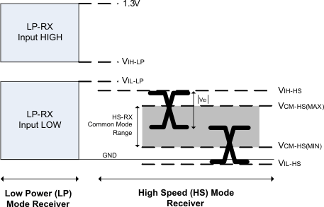
 Figure 1. DSI Receiver Voltage Definitions
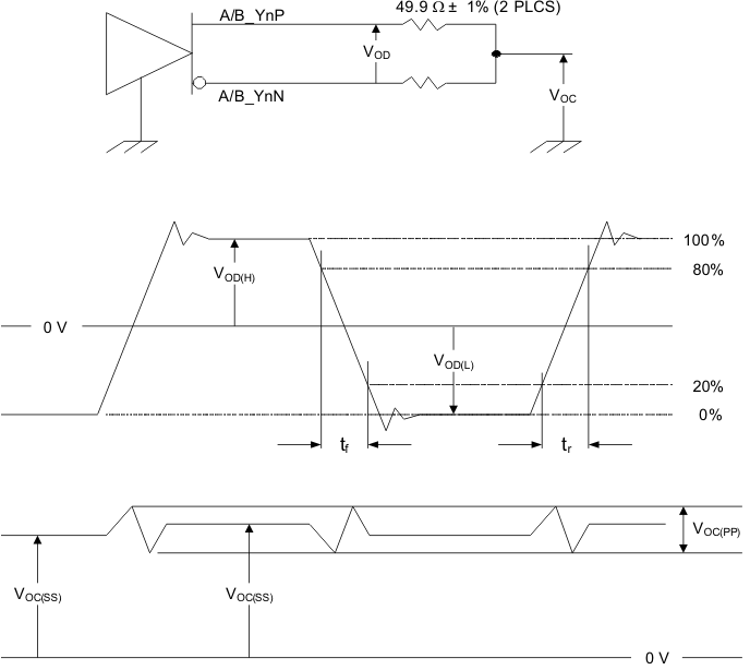
  Figure 2. Test Load and Voltage Definitions for Flatlink Outputs
1. See the ULPS section of the data sheet for the ULPS entry and exit sequence.
2. ULPS entry and exit protocol and timing requirements must be met per MIPI® DPHY specification.
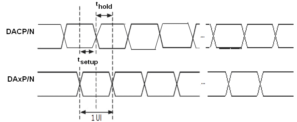
Figure 3. ULPS Timing Definition  Figure 4. DSI HS Mode Receiver Timing Definitions
  Figure 5. SN65DSI84 Flatlink Timing Definitions