JAJSFO1G September   2012  – June 2018 SN65DSI84

PRODUCTION DATA.  

  1. 特長
  2. アプリケーション
  3. 概要
    1.     標準アプリケーション
  4. 改訂履歴
  5. Pin Configuration and Functions
    1.     Pin Functions
  6. Specifications
    1. 6.1 Absolute Maximum Ratings
    2. 6.2 EDS Ratings
    3. 6.3 Recommended Operating Conditions
    4. 6.4 Thermal Information
    5. 6.5 Electrical Characteristics
    6. 6.6 Switching Characteristics
  7. Detailed Description
    1. 7.1 Overview
    2. 7.2 Functional Block Diagram
    3. 7.3 Feature Description
      1. 7.3.1 Clock Configurations and Multipliers
      2. 7.3.2 ULPS
      3. 7.3.3 LVDS Pattern Generation
    4. 7.4 Device Functional Modes
      1. 7.4.1 Reset Implementation
      2. 7.4.2 Initialization Sequence
      3. 7.4.3 LVDS Output Formats
      4. 7.4.4 DSI Lane Merging
      5. 7.4.5 DSI Pixel Stream Packets
      6. 7.4.6 DSI Video Transmission Specifications
      7. 7.4.7 Operating Modes
    5. 7.5 Programming
      1. 7.5.1 Local I2C Interface Overview
    6. 7.6 Register Maps
      1. 7.6.1 Control and Status Registers Overview
  8. Application and Implementation
    1. 8.1 Application Information
      1. 8.1.1 Video Stop and Restart Sequence
      2. 8.1.2 Reverse LVDS Pin Order Option
      3. 8.1.3 IRQ Usage
    2. 8.2 Typical Application
      1. 8.2.1 Design Requirements
      2. 8.2.2 Detailed Design Procedure
        1. 8.2.2.1 Example Script
      3. 8.2.3 Application Curve
  9. Power Supply Recommendations
    1. 9.1 VCC Power Supply
    2. 9.2 VCORE Power Supply
  10. 10Layout
    1. 10.1 Layout Guidelines
      1. 10.1.1 Package Specific
      2. 10.1.2 Differential Pairs
      3. 10.1.3 Ground
    2. 10.2 Layout Example
  11. 11デバイスおよびドキュメントのサポート
    1. 11.1 ドキュメントの更新通知を受け取る方法
    2. 11.2 コミュニティ・リソース
    3. 11.3 商標
    4. 11.4 静電気放電に関する注意事項
    5. 11.5 Glossary
  12. 12メカニカル、パッケージ、および注文情報

パッケージ・オプション

メカニカル・データ(パッケージ|ピン)
サーマルパッド・メカニカル・データ
発注情報

LVDS Output Formats

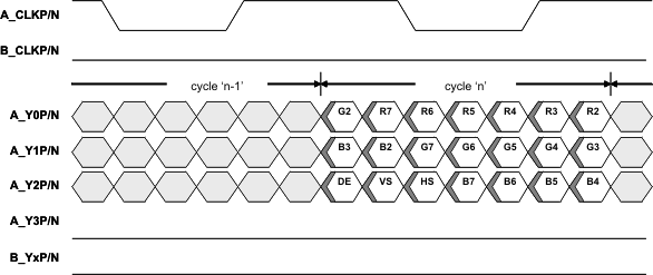
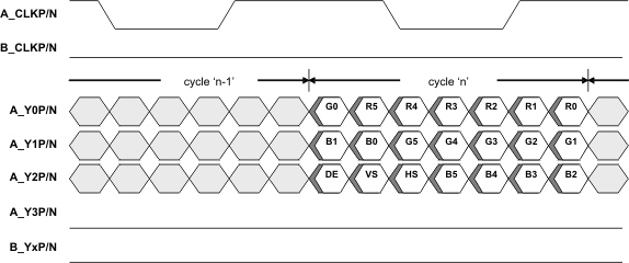
The SN65DSI84 processes DSI packets and produces video data driven to the FlatLink™ LVDS interface in an industry standard format. Single-Link LVDS and Dual-Link LVDS are supported by the SN65DSI84; when the FlatLink™ output is implemented in a Dual-Link configuration, channel A carries the odd pixel data, and channel B carries the even pixel data. During conditions such as the default condition, and some video synchronization periods, where no video stream data is passing from the DSI input to the LVDS output, the SN65DSI84 transmits zero value pixel data on the LVDS outputs while maintaining transmission of the vertical sync and horizontal sync status.

Figure 9 illustrates a Single-Link LVDS 18bpp application.

Figure 10 illustrates a Dual-Link 24 bpp application using Format 2, controlled by CHA_24BPP_FORMAT1 (CSR 0x18.1) and CHB_24BPP_FORMAT1 (CSR 0x18.0). In data Format 2, the two MSB per color are transferred on the Y3P/N LVDS lane.

Figure 11 illustrates a 24 bpp Single-Link application using Format 1. In data Format 1, the two LSB per color are transferred on the Y3P/N LVDS lane.

Figure 12 illustrates a Single-Link LVDS application where 24 bpp data is received from DSI and converted to 18 bpp data for transmission to an 18 bpp panel. This application is configured by setting CHA_24BPP_FORMAT1 (CSR 0x18.1) to ‘1’ and CHA_24BPP_MODE (CSR 0x18.3) to ‘0’. In this configuration, the SN65DSI84 will not transmit the 2 LSB per color since the Y3P/N LVDS lane is disabled.

NOTE

Note: Figure 9, Figure 10, Figure 11, and Figure 12 only illustrate a few example applications for the SN65DSI84. Other applications are also supported.
SN65DSI84 fig4_flatlink_LLSEB9.gif
DE = Data Enable; Channel B Clock, Channel B Data, and A_Y3P/N are Output Low
Figure 9. Flatlink Output Data; Single-Link 18 Bpp
SN65DSI84 fig5_flatlink_LLSEB9.gif
DE = Data Enable; (o) = Odd Pixels; (e) = Even Pixels
Figure 10. Flatlink Output Data (Format 2); Dual-Link 24 Bpp
SN65DSI84 fig6_flatlink_LLSEB9.gif
DE = Data Enable; Channel B Clock and Data are Output Low
Figure 11. Flatlink Output Data (Format 1); Single-Link 24 Bpp
SN65DSI84 fig7_flatlink_LLSEB9.gif
DE = Data Enable; Channel B Clock, Channel B Data, and A_Y3P/N a re Output Low; Channel B Clock, Channel B Data, and A_Y3P/N are Output Low
Figure 12. Flatlink Output Data (Format 1); 24-Bpp to Single-Link 18-Bpp Conversion