SLLSEJ5A July 2014 – December 2015 SN65DSI86-Q1
PRODUCTION DATA.
- 1 Features
- 2 Applications
- 3 Description
- 4 Revision History
- 5 Description (continued)
- 6 Pin Configuration and Functions
- 7 Specifications
-
8 Detailed Description
- 8.1 Overview
- 8.2 Functional Block Diagram
- 8.3 Feature Description
- 8.4
Device Functional Modes
- 8.4.1 Reset Implementation
- 8.4.2 Power-Up Sequence
- 8.4.3 Power Down Sequence
- 8.4.4 Display Serial Interface (DSI)
- 8.4.5
DisplayPort
- 8.4.5.1 HPD (Hot Plug/Unplug Detection)
- 8.4.5.2 AUX_CH
- 8.4.5.3 I2C-Over-AUX
- 8.4.5.4 DisplayPort PLL
- 8.4.5.5 DP Output VOD and Pre-emphasis Settings
- 8.4.5.6 DP Main Link Configurability
- 8.4.5.7 DP Main Link Training
- 8.4.5.8 Panel Size vs DP Configuration
- 8.4.5.9 Panel Self Refresh (PSR)
- 8.4.5.10 Secondary Data Packet (SDP)
- 8.4.5.11 Color Bar Generator
- 8.4.5.12 DP Pattern
- 8.4.5.13 BPP Conversion
- 8.5 Programming
- 8.6 Register Map
- 9 Application and Implementation
- 10Power Supply Recommendations
- 11Layout
- 12Device and Documentation Support
- 13Mechanical, Packaging, and Orderable Information
パッケージ・オプション
メカニカル・データ(パッケージ|ピン)
- PAP|64
サーマルパッド・メカニカル・データ
- PAP|64
発注情報
9 Application and Implementation
NOTE
Information in the following applications sections is not part of the TI component specification, and TI does not warrant its accuracy or completeness. TI’s customers are responsible for determining suitability of components for their purposes. Customers should validate and test their design implementation to confirm system functionality
9.1 Application Information
The SN65DSIx6 is a bridge which interfaces DSI to embedded DisplayPort (eDP). Because it does not support HDCP, it is only intended for internal applications like notebooks and tablets. Four lanes of HBR2 (17.28 Gbps before 8b10b encoding) and dual DSI input (up to 8 lanes at 1.5 Gbps for a total of 12 Gbps) allows the SN65DSIx6 to support large high resolution eDP panels.
9.2 Typical Application
9.2.1 1080p (1920x1080 60 Hz) Panel
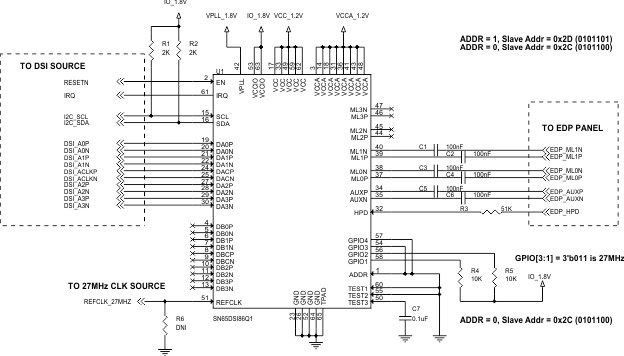
 Figure 20. 1080p (1920 × 1080 60 Hz) Panel
9.2.1.1 Design Requirements
For this design example, use the parameters listed in Table 34.
Table 34. Design Parameters
| DESIGN PARAMETER | EXAMPLE VALUE | |||
|---|---|---|---|---|
| VCC and VCCA Supply | 1.2 V (± 5%) | |||
| VCCIO Supply | 1.8 V (± 10%) | |||
| VPLL Supply | 1.8 V (± 10%) | |||
| Clock Source (REFCLK or DSIA_CLK) | REFCLK | |||
| REFCLK Frequency (12 MHz, 19.2 MHz, 26 MHz, 27 MHz, or 38.4 MHz) | 27 MHz | |||
| DSIA Clock Frequency | N/A | |||
| eDP PANEL EDID RESOLUTION INFORMATION | ||||
| Pixel Clock (MHz) | 148.5 | |||
| Horizontal Active (pixels) | 1920 | |||
| Horizontal Blanking (pixels) | 280 | |||
| Vertical Active (lines) | 1080 | |||
| Vertical Blanking (lines) | 45 | |||
| Horizontal Sync Offset (pixels) | 88 | |||
| Horizontal Sync Pulse Width (pixels) | 44 | |||
| Vertical Sync Offset (lines) | 4 | |||
| Vertical Sync Pulse Width (lines) | 5 | |||
| Horizontal Sync Pulse Polarity | Positive | |||
| Vertical Sync Pulse Polarity | Positive | |||
| Color Bit Depth (6 bpc or 8 bpc) | 8 (24 bpp) | |||
| eDP PANEL DPCD INFORMATION | ||||
| eDP Version (1.0, 1.1, 1.2, 1.3, or 1.4) | 1.3 | |||
| Number of eDP lanes (1, 2, or 4) | 2 | |||
| Datarate Supported (1.62 Gbps, 2.16 Gbps, 2.43 Gbps, 2.70 Gbps, 3.24 Gbps, 4.32 Gbps, or 5.40 Gbps) | 2.70 | |||
| DSI INFORMATION | ||||
| APU or GPU Maximum number of DSI Lanes (1 through 8) | 4 | |||
| APU or GPU Maximum DSI Clock Frequency (MHz) | 500 | |||
| Single or Dual DSI | Single | |||
| Dual DSI Configuration (Odd/Even or Left/Right) | NA | |||
9.2.1.2 Detailed Design Procedure
9.2.1.2.1 eDP Design Procedure
The panel, as indicated by the panel EDID information, supports a pixel clock of 148.5 MHz at 8 bpc or 24 bpp. This translates to a stream bit rate of 3.564 Gbps.
| Stream Bit Rate = PixelClock × bpp | ||
| Stream Bit Rate = 148.5 × 24 | ||
| Stream Bit Rate = 3.564 Gbps |
In order to support the panel stream bit rate, the SN65DSIx6 eDP interface must be programmed so that the total eDP data rate is greater than the stream bit rate. In this example, the total eDP data rate is calculated as:
| eDP Total Bit Rate = #_of_eDP_Lanes × DataRate × 0.80 | ||
| eDP Total Bit Rate = 2 × 2.7 Gbps × 0.80 | ||
| eDP Total Bit Rate = 4.32 Gbps. |
In this example, the eDP panel DPCD registers indicates eDP1.3 compliant, supports a data rate of 2.7 Gbps per lane, and a lane count of 2. For this panel to operate properly, the SN65DSIx6 would need to be programmed to enable two lanes at a data rate of 2.7 Gbps each.
In portable and mobile applications, total power consumption is a key care-about. In this example, the panel chosen is eDP 1.3 compliant and supports a data rate of 2.7 Gbps per lane. The SN65DSIx6 power consumption is a function of the data rate and number of active DP lanes. By reducing the number of active lanes and/or data rate, the total power consumption of the SN65DSIx6 is reduced as well. If a panel which supported data rate of 5.4 Gbps was chosen over the example panel, the number of lanes could be reduced from two lanes to one lane. Or if a panel which was eDP1.4 compliant and support 2.43 Gbps data rate was chosen over the example panel, the data rate could be reduced from 2.7 Gbps to 2.43 Gbps.
Once the eDP interface parameters are known, the video resolution parameters required by the panel need to be programmed into the SN65DSIx6. For this example, the parameters programmed would be the following:
| Horizontal Active = 1920 or 0x780 | ||
| CHA_ACTIVE_LINE_LENGTH_LOW = 0x80 | ||
| CHA_ACTIVE_LINE_LENGTH_HIGH = 0x07 |
| Vertical Active = 1080 or 0x438 | ||
| CHA_VERTICAL_DISPLAY_SIZE_LOW = 0x38 | ||
| CHA_VERTICAL_DISPLAY_SIZE_HIGH = 0x04 |
| Horizontal Pulse Width = 44 or 0x2C | ||
| HORIZONTAL_PULSE_WIDTH_LOW = 0x2C | ||
| HORIZONTAL_PULSE_WIDTH_HIGH = 0x00 |
| Vertical Pulse Width = 5 | ||
| VERTICAL_PULSE_WIDTH_LOW = 0x05 | ||
| VERTICAL_PULSE_WIDTH_HIGH = 0x00 |
| Horizontal Backporch = HorizontalBlanking – (HorizontalSyncOffset + HorizontalSyncPulseWidth) | ||
| Horizontal Backporch = 280 – (88 + 44) | ||
| CHA_HORIZONTAL_BACK_PORCH = 0x94 | ||
| Horizontal Backporch = 148 or 0x94 |
| Vertical Backporch = VerticalBlanking – (VerticalSyncOffset + VerticalSyncPulseWidth) | ||
| Vertical Backporch = 45 – (4 + 5) | ||
| Vertical Backporch = 36 or 0x24 | ||
| CHA_VERTICAL_BACK_PORCH = 0x24 |
| Horizontal Frontporch = HorizontalSyncOffset | ||
| Horizontal Frontporch = 88 or 0x58 | ||
| CHA_HORIZONTAL_FRONT_PORCH = 0x58 |
| Vertical Frontporch = VerticalSyncOffset | ||
| Vertical Frontporch = 4 | ||
| CHA_VERTICAL_FRONT_PORCH = 0x04 |
9.2.1.2.2 DSI Design Procedure
The APU or GPU must provide a stream bit rate as required by the eDP panel. In this particular example, the eDP panel stream rate is 3.564 Gbps. Because the SN65DSIx6 can support a DSI clock rate of up to 750 MHz (or 1.5 Gbps), the minimum number of required DSI lanes to meet the stream bit rate is three lanes. But in this example, the APU/GPU maximum DSI Clock frequency is 500 MHz. This means the number of required DSI lanes will need to be increased to four lanes.
| Min number of DSI Lanes = StreamBitRate / MaxDSIClock | ||
| Min number of DSI Lanes = 3564 MBps / (500 × 2) | ||
| Min number of DSI Lanes = 3.564 lanes | ||
| Min number of DSI Lanes = 4 lanes |
After determining the number of required DSI lanes, the next step is to determine the minimum required DSI clock frequency to support the stream bit rate of the eDP panel. For 24 bpp, the calculation for determining the DSI clock frequency is as follows:
| Min Required DSI Clock Frequency = StreamBitRate / (Min_Number_DSI_Lanes × 2) | ||
| Min Required DSI Clock Frequency = 3564 / (4 × 2) | ||
| Min Required DSI Clock Frequency = 445.5 MHz |
In this example, the clock source for the SN65DSIx6 is the REFCLK pin. When using the REFCLK as the clock source, any DSI Clock frequency is supported. But if the clock source was instead the DSI A clock, then the required DSI Clock frequency would need to change to a frequency supported by the SN65DSIx6. When operating in this mode, any one of the following DSI A clock frequencies can be used: 384 MHz, 416 MHz, 460.8 MHz, 468 MHz, or 486 MHz. In most cases, a eDP panel would support some variation from the ideal pixel clock frequency. For this example either 416 MHz or 460.8 MHz could be tried.
| The DSI mode, number of lanes, and DSI Clock frequency needs to be programmed into the SN65DSIx6. | ||
| DSI_CHANNEL_MODE = 1 (Single DSI Channel) | ||
| CHA_DSI_LANES = 3 (for 4 lanes) | ||
| CHA_DSI_CLK_RANGE = 0x59 (equates to 445 MHz) | ||
| REFCLK_FREQ = 0x06 (27 MHz) |
9.2.1.2.3 Example Script
This example configures the SN65DSIx6 for the following configuration:
<aardvark>
<configure i2c="1" spi="1" gpio="0" tpower="1" pullups="0" />
<i2c_bitrate khz="100" />

======REFCLK 27MHz ======
<i2c_write addr="0x2D" count="1" radix="16">0A 06</i2c_write> />

======Single 4 DSI lanes======
<i2c_write addr="0x2D" count="1" radix="16">10 26</i2c_write> />

======DSIA CLK FREQ 445MHz======
<i2c_write addr="0x2D" count="1" radix="16">12 59</i2c_write> />

======enhanced framing and ASSR======
<i2c_write addr="0x2D" count="1" radix="16">5A 05</i2c_write> />

======2 DP lanes no SSC======
<i2c_write addr="0x2D" count="1" radix="16">93 20</i2c_write> />

======HBR (2.7Gbps)======
<i2c_write addr="0x2D" count="1" radix="16">94 80</i2c_write> />

======PLL ENABLE======
<i2c_write addr="0x2D" count="1" radix="16">0D 01</i2c_write> <sleep ms="10" />

======Verify PLL is locked======
<i2c_write addr="0x2D" count="0" radix="16">0A</i2c_write> />
<i2c_read addr="0x2D" count="2" radix="16">00</i2c_read> <sleep ms="10" />

======POST-Cursor2 0dB ======
<i2c_write addr="0x2D" count="1" radix="16">95 00</i2c_write> />

======Write DPCD Register 0x0010A in Sink to Enable ASSR======
<i2c_write addr="0x2D" count="1" radix="16">64 01</i2c_write> />
<i2c_write addr="0x2D" count="1" radix="16">74 00</i2c_write> />
<i2c_write addr="0x2D" count="1" radix="16">75 01</i2c_write> />
<i2c_write addr="0x2D" count="1" radix="16">76 0A</i2c_write> />
<i2c_write addr="0x2D" count="1" radix="16">77 01</i2c_write> />
<i2c_write addr="0x2D" count="1" radix="16">78 81</i2c_write> <sleep ms="10" />

======Semi-Auto TRAIN ======
<i2c_write addr="0x2D" count="1" radix="16">96 0A</i2c_write> <sleep ms="20" />

======Verify Training was successful======
<i2c_write addr="0x2D" count="0" radix="16">96</i2c_write> />
<i2c_read addr="0x2D" count="1" radix="16">00</i2c_read> <sleep ms="10" />

=====CHA_ACTIVE_LINE_LENGTH is 1920 =======
<i2c_write addr="0x2D" count="2" radix="16">20 80 07</i2c_write> />

=====CHA_VERTICAL_DISPLAY_SIZE is 1080 =======
<i2c_write addr="0x2D" count="2" radix="16">24 38 04</i2c_write> />

=====CHA_HSYNC_PULSE_WIDTH is 44 positive =======
<i2c_write addr="0x2D" count="2" radix="16">2C 2C 00</i2c_write> />

=====CHA_VSYNC_PULSE_WIDTH is 5 positive=======
<i2c_write addr="0x2D" count="2" radix="16">30 05 80</i2c_write> />

=====CHA_HORIZONTAL_BACK_PORCH is 148=======
<i2c_write addr="0x2D" count="1" radix="16">34 94</i2c_write> />

=====CHA_VERTICAL_BACK_PORCH is 36=======
<i2c_write addr="0x2D" count="1" radix="16">36 24</i2c_write> />

=====CHA_HORIZONTAL_FRONT_PORCH is 88=======
<i2c_write addr="0x2D" count="1" radix="16">38 58</i2c_write> />

=====CHA_VERTICAL_FRONT_PORCH is 4=======
<i2c_write addr="0x2D" count="1" radix="16">3A 04</i2c_write> />

======DP- 24bpp======
<i2c_write addr="0x2D" count="1" radix="16">5B 00</i2c_write> />

=====COLOR BAR disabled=======
<i2c_write addr="0x2D" count="1" radix="16">3C 00</i2c_write> />

======enhanced framing, ASSR, and Vstream enable======
<i2c_write addr="0x2D" count="1" radix="16">5A 0D</i2c_write> />

</aardvark>
9.2.1.3 Application Curve
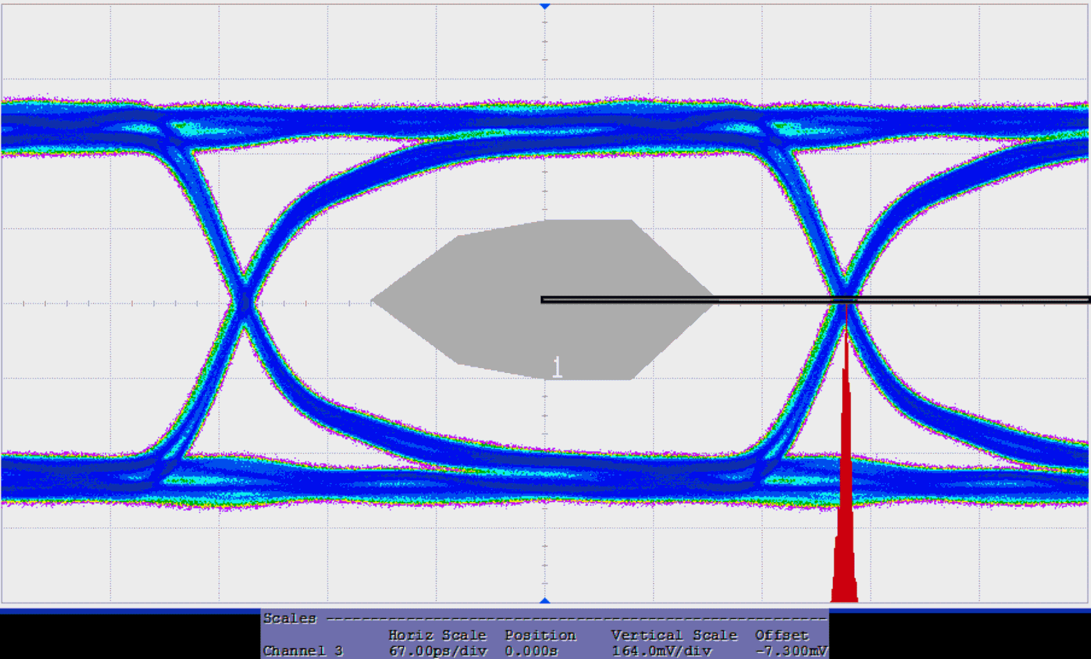
 Figure 21. HBR Eye Diagram