SLLSEJ5A July 2014 – December 2015 SN65DSI86-Q1
PRODUCTION DATA.
- 1 Features
- 2 Applications
- 3 Description
- 4 Revision History
- 5 Description (continued)
- 6 Pin Configuration and Functions
- 7 Specifications
-
8 Detailed Description
- 8.1 Overview
- 8.2 Functional Block Diagram
- 8.3 Feature Description
- 8.4
Device Functional Modes
- 8.4.1 Reset Implementation
- 8.4.2 Power-Up Sequence
- 8.4.3 Power Down Sequence
- 8.4.4 Display Serial Interface (DSI)
- 8.4.5
DisplayPort
- 8.4.5.1 HPD (Hot Plug/Unplug Detection)
- 8.4.5.2 AUX_CH
- 8.4.5.3 I2C-Over-AUX
- 8.4.5.4 DisplayPort PLL
- 8.4.5.5 DP Output VOD and Pre-emphasis Settings
- 8.4.5.6 DP Main Link Configurability
- 8.4.5.7 DP Main Link Training
- 8.4.5.8 Panel Size vs DP Configuration
- 8.4.5.9 Panel Self Refresh (PSR)
- 8.4.5.10 Secondary Data Packet (SDP)
- 8.4.5.11 Color Bar Generator
- 8.4.5.12 DP Pattern
- 8.4.5.13 BPP Conversion
- 8.5 Programming
- 8.6 Register Map
- 9 Application and Implementation
- 10Power Supply Recommendations
- 11Layout
- 12Device and Documentation Support
- 13Mechanical, Packaging, and Orderable Information
パッケージ・オプション
メカニカル・データ(パッケージ|ピン)
- PAP|64
サーマルパッド・メカニカル・データ
- PAP|64
発注情報
11 Layout
11.1 Layout Guidelines
To minimize the power supply noise floor, provide good decoupling near the SN65DSIx6 power pins. The use of four ceramic capacitors (2 × 0.1 μF and 2 × 0.1 μF) provides good performance. At the very least, TI recommends to install one 0.1-μF and one 0.01-μF capacitors near the SN65DSIx6. To avoid large current loops and trace inductance, the trace length between decoupling capacitor and device power inputs pins must be minimized. Placing the capacitor underneath the SN65DSIx6 on the bottom of the PCB is often a good choice.
Note: The power supplies VPLL, VCCIO, VCCA, and VCC can be applied simultaneously.
11.1.1 DSI Guidelines
- DA*P/N and DB*P/N pairs should be routed with controlled 100-Ω differential impedance (± 20%) or 50-Ω single-ended impedance (±15%).
- Keep away from other high speed signals.
- Keep lengths to within 5 mils of each other.
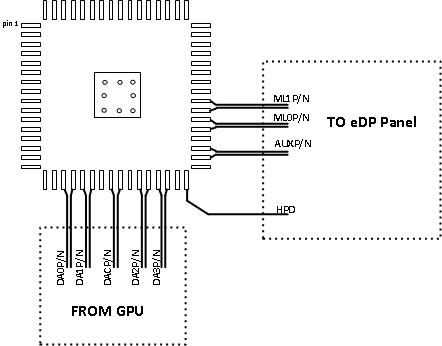
- Length matching should be near the location of mismatch. See Figure 4 for an example.
- Each pair should be separated at least by 3 times the signal trace width.
- The use of bends in differential traces should be kept to a minimum. When bends are used, the number of left and right bends should be as equal as possible and the angle of the bend should be ≥ 135°. This arrangement minimizes any length mismatch caused by the bends and therefore minimizes the impact that bends have on EMI.
- Route all differential pairs on the same of layer.
- The number of VIAS should be kept to a minimum. TI recommends to keep the VIAS count to 2 or less.
- Keep traces on layers adjacent to ground plane.
- Do NOT route differential pairs over any plane split.
- Adding Test points will cause impedance discontinuity and will therefore negatively impact signal performance. If test points are used, they should be placed in series and symmetrically. They must not be placed in a manner that causes a stub on the differential pair.
- The maximum trace length over FR4 between SN65DSI86 and the GPU is 25 to 30 cm.
11.1.2 eDP Guidelines
- ML*P/N pairs should be routed with controlled 100-Ω differential impedance (± 20%) or 50-Ω single-ended impedance (± 15%).
- Keep away from other high speed signals.
- Keep lengths to within 5 mils of each other.
- Length matching should be near the location of mismatch. See Figure 4 for an example.
- Each pair should be separated at least by 3 times the signal trace width.
- The use of bends in differential traces should be kept to a minimum. When bends are used, the number of left and right bends should be as equal as possible and the angle of the bend should be ≥ 135°. This arrangement minimizes any length mismatch caused by the bends and therefore minimizes the impact that bends have on EMI
- Route all differential pairs on the same of layer.
- The number of VIAS should be kept to a minimum. TI recommends to keep the VIAS count to 2 or less.
- Keep traces on layers adjacent to ground plane.
- Do NOT route differential pairs over any plane split.
- Adding Test points will cause impedance discontinuity and will therefore negatively impact signal performance. If test points are used, they should be placed in series and symmetrically. They must not be placed in a manner that causes a stub on the differential pair.
- The maximum trace length over FR4 between SN65DSIx6 and the eDP receptacle is 4 inches for data rates less than or equal to HBR (2.7 Gbps) and 2 inches for HBR2 (5.4 Gbps).
11.1.3 Ground
TI recommends that only one board ground plane be used in the design. This provides the best image plane for signal traces running above the plane. The thermal pad of the SN65DSIx6 should be connected to this plane with vias.
11.2 Layout Example
