JAJSQ80C september   2013  – october 2020 SN65DSI86

PRODUCTION DATA  

  1.   1
  2. 特長
  3. アプリケーション
  4. 概要
  5. Revision History
  6. Description (continued)
  7. Pin Configuration and Functions
  8. Specifications
    1. 7.1 Absolute Maximum Ratings
    2. 7.2 ESD Ratings
    3. 7.3 Recommended Operating Conditions
    4. 7.4 Thermal Information
    5. 7.5 Electrical Characteristics
    6. 7.6 Timing Requirements
    7. 7.7 Switching Characteristics
  9. Detailed Description
    1. 8.1 Overview
    2. 8.2 Functional Block Diagram
    3. 8.3 Feature Description
      1. 8.3.1 MIPI Dual DSI Interface
      2. 8.3.2 Embedded DisplayPort Interface
      3. 8.3.3 General-Purpose Input and Outputs
        1. 8.3.3.1 GPIO REFCLK and DSIA Clock Selection
        2. 8.3.3.2 Suspend Mode
        3. 8.3.3.3 Pulse Width Modulation (PWM)
    4. 8.4 Device Functional Modes
      1. 8.4.1 Reset Implementation
      2. 8.4.2 Power-Up Sequence
      3. 8.4.3 Power Down Sequence
      4. 8.4.4 Display Serial Interface (DSI)
        1. 8.4.4.1 DSI Lane Merging
        2. 8.4.4.2 DSI Supported Data Types
        3. 8.4.4.3 Generic Request Datatypes
          1. 8.4.4.3.1 Generic Read Request 2-Parameters Request
          2. 8.4.4.3.2 Generic Short Write 2-Parameters Request
          3. 8.4.4.3.3 Generic Long Write Packet Request
        4. 8.4.4.4 DSI Pixel Stream Packets
        5. 8.4.4.5 DSI Video Transmission Specifications
        6. 8.4.4.6 Video Format Parameters
        7. 8.4.4.7 GPU LP-TX Clock Requirements
      5. 8.4.5 DisplayPort
        1. 8.4.5.1  HPD (Hot Plug/Unplug Detection)
        2. 8.4.5.2  AUX_CH
          1. 8.4.5.2.1 Native Aux Transactions
        3. 8.4.5.3  I2C-Over-AUX
          1. 8.4.5.3.1 Direct Method (Clock Stretching)
          2. 8.4.5.3.2 Indirect Method (CFR Read/Write)
        4. 8.4.5.4  DisplayPort PLL
        5. 8.4.5.5  DP Output VOD and Pre-emphasis Settings
        6. 8.4.5.6  DP Main Link Configurability
        7. 8.4.5.7  DP Main Link Training
          1. 8.4.5.7.1 Manual Link Training
          2. 8.4.5.7.2 Fast Link Training
          3. 8.4.5.7.3 54
          4. 8.4.5.7.4 Semi-Auto Link Training
          5. 8.4.5.7.5 Redriver Semi-Auto Link Training
        8. 8.4.5.8  Panel Size vs DP Configuration
        9. 8.4.5.9  Panel Self Refresh (PSR)
        10. 8.4.5.10 Secondary Data Packet (SDP)
        11. 8.4.5.11 Color Bar Generator
        12. 8.4.5.12 DP Pattern
          1. 8.4.5.12.1 HBR2 Compliance Eye
          2. 8.4.5.12.2 80-Bit Custom Pattern
        13. 8.4.5.13 BPP Conversion
    5. 8.5 Programming
      1. 8.5.1 Local I2C Interface Overview
    6. 8.6 Register Map
      1. 8.6.1 Standard CFR Registers (PAGE 0)
  10. Application and Implementation
    1. 9.1 Application Information
    2. 9.2 Typical Application
      1. 9.2.1 1080p (1920x1080 60 Hz) Panel
        1. 9.2.1.1 Design Requirements
        2. 9.2.1.2 Detailed Design Procedure
          1. 9.2.1.2.1 eDP Design Procedure
          2. 9.2.1.2.2 76
          3. 9.2.1.2.3 DSI Design Procedure
          4. 9.2.1.2.4 78
          5. 9.2.1.2.5 Example Script
        3. 9.2.1.3 Application Curve
  11. 10Power Supply Recommendations
    1. 10.1 VCC Power Supply
    2. 10.2 VCCA Power supply
    3. 10.3 VPLL and VCCIO Power Supplies
  12. 11Layout
    1. 11.1 Layout Guidelines
      1. 11.1.1 DSI Guidelines
      2. 11.1.2 eDP Guidelines
      3. 11.1.3 Ground
    2. 11.2 Layout Example
  13. 12Device and Documentation Support
    1. 12.1 Documentation Support
      1. 12.1.1 Related Documentation
    2. 12.2 Receiving Notification of Documentation Updates
    3. 12.3 Community Resources
    4. 12.4 Trademarks
  14. 13Mechanical, Packaging, and Orderable Information

パッケージ・オプション

メカニカル・データ(パッケージ|ピン)
サーマルパッド・メカニカル・データ
発注情報

Reset Implementation

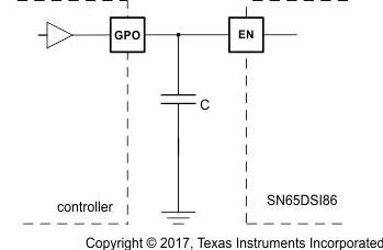
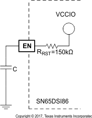
When EN is deasserted, CMOS inputs are ignored, the MIPI D-PHY inputs are disabled, and outputs are high impedance. It is critical to transition the EN input from a low to a high level after the VCC supply has reached the minimum recommended operating voltage. This is achieved by a control signal to the EN input, or by an external capacitor connected between EN and GND. To insure that the SN65DSI86 is properly reset, the EN pin must be deasserted for at least 100 µs before being asserted.

When implementing the external capacitor, the size of the external capacitor depends on the power up ramp of the VCC supply, where a slower ramp-up results in a larger value external capacitor. See the latest reference schematic for the SN65DSI86 device and/or consider approximately 200-nF capacitor as a reasonable first estimate for the size of the external capacitor.

Both EN implementations are shown in Figure 8-1 and Figure 8-2.
GUID-025AE25A-6C2E-4B6A-986D-C4524AA689D0-low.gif
Figure 8-1 External Capacitor Controlled EN
GUID-AE26172F-2EF5-4AD2-861A-68A23B06DF6E-low.gif
Figure 8-2 EN Input from Active Controller