JAJSQ80C september 2013 – october 2020 SN65DSI86
PRODUCTION DATA
- 1
- 1 特長
- 2 アプリケーション
- 3 概要
- 4 Revision History
- 5 Description (continued)
- 6 Pin Configuration and Functions
- 7 Specifications
-
8 Detailed Description
- 8.1 Overview
- 8.2 Functional Block Diagram
- 8.3 Feature Description
- 8.4
Device Functional Modes
- 8.4.1 Reset Implementation
- 8.4.2 Power-Up Sequence
- 8.4.3 Power Down Sequence
- 8.4.4 Display Serial Interface (DSI)
- 8.4.5
DisplayPort
- 8.4.5.1 HPD (Hot Plug/Unplug Detection)
- 8.4.5.2 AUX_CH
- 8.4.5.3 I2C-Over-AUX
- 8.4.5.4 DisplayPort PLL
- 8.4.5.5 DP Output VOD and Pre-emphasis Settings
- 8.4.5.6 DP Main Link Configurability
- 8.4.5.7 DP Main Link Training
- 8.4.5.8 Panel Size vs DP Configuration
- 8.4.5.9 Panel Self Refresh (PSR)
- 8.4.5.10 Secondary Data Packet (SDP)
- 8.4.5.11 Color Bar Generator
- 8.4.5.12 DP Pattern
- 8.4.5.13 BPP Conversion
- 8.5 Programming
- 8.6 Register Map
- 9 Application and Implementation
- 10Power Supply Recommendations
- 11Layout
- 12Device and Documentation Support
- 13Mechanical, Packaging, and Orderable Information
7.7 Switching Characteristics
over operating free-air temperature range (unless otherwise noted)
| PARAMETER | TEST CONDITIONS | MIN | TYP(1) | MAX | UNIT | |
|---|---|---|---|---|---|---|
| MIPI DSI INTERFACE | ||||||
| tGS | DSI LP glitch suppression pulse width | 300 | ps | |||
| tHS-SETUP | DSI HS data to clock setup time | 0.2 | UI | |||
| tHS-HOLD | DSI HS clock to data hold time | 0.2 | UI | |||
| DisplayPort MAIN LINK | ||||||
| FBR7 | Bit rate 7 | 5.37138 | 5.4 | 5.40162 | Gbps | |
| FBR6 | Bit rate 6 | 4.297104 | 4.32 | 4.321296 | Gbps | |
| FBR5 | Bit rate 5 | 3.222828 | 3.24 | 3.240972 | Gbps | |
| FBR4 | Bit rate 4 | 2.68569 | 2.7 | 2.70081 | Gbps | |
| FBR3 | Bit rate 3 | 2.417121 | 2.43 | 2.430729 | Gbps | |
| FBR2 | Bit rate 2 | 2.148552 | 2.16 | 2.160648 | Gbps | |
| FBR1 | Bit rate 1 | 1.611414 | 1.62 | 1.620486 | Gbps | |
| UIBR7 | Unit interval for BR7 | High limit = +300 ppm. Low limit = –5300 ppm | 185 | ps | ||
| UIBR6 | Unit interval for BR6 | High limit = +300 ppm. Low limit = –5300 ppm | 231.5 | ps | ||
| UIBR5 | Unit interval for BR5 | High limit = +300 ppm. Low limit = –5300 ppm | 308.6 | ps | ||
| UIBR4 | Unit interval for BR4 | High limit = +300 ppm. Low limit = –5300 ppm | 370.4 | ps | ||
| UIBR3 | Unit interval for BR3 | High limit = +300 ppm. Low limit = –5300 ppm | 411.5 | ps | ||
| UIBR2 | Unit interval for BR2 | High limit = +300 ppm. Low limit = –5300 ppm | 463 | ps | ||
| UIBR1 | Unit interval for BR1 | High limit = +300 ppm. Low limit = –5300 ppm | 617.3 | ps | ||
| tERC_L0 | Differential output rise or fall time with DP_ERC set to 0 | 50 | 61 | 80 | ps | |
| tERC_L1 | Differential output rise or fall time with DP_ERC set to 1 | 74 | 95 | 115 | ps | |
| tERC_L2 | Differential output rise or fall time with DP_ERC set to 2 | 108 | 123 | 146 | ps | |
| tERC_L3 | Differential output rise or fall time with DP_ERC set to 3 | 136 | 153 | 168 | ps | |
| tTX_RISE_FALL _MISMATCH | Lane intra-pair output skew at TX pins | 5% | ||||
| tINTRA_SKEW | Intra-pair differential skew | 20 | ps | |||
| tINTER_SKEW | Inter-pair differential skew | 100 | ps | |||
| tTX_EYE_HBR2 | Minimum TX eye width at TX package pins for HBR2(2) | 0.73 | UIHBR2 | |||
| tTX_EYE_MED_TO _MAX_JIT_HBR2 | Maximum time between the jitter median and maximum deviation from the median at TX package pins for HBR2(2) | 0.135 | UIHBR2 | |||
| tTX_EYE_HBR | Minimum TX eye width at TX package pins for HBR(2) | 0.72 | UIHBR | |||
| tTX_EYE_MED_TO _MAX_JIT_HBR | Maximum time between the jitter median and maximum deviation from the median at TX package pins for HBR(2) | 0.147 | UIHBR | |||
| tTX_EYE_RBR | Minimum TX eye width at TX package pins for RBR(2) | 0.82 | UIRBR | |||
| tTX_EYE_MED_TO _MAX_JIT_RBR | Maximum time between the jitter median and maximum deviation from the median at TX package pins for RBR(2) | 0.09 | UIRBR | |||
| tXSSC_AMP | Link clock down-spreading | 0% | 0.5% | |||
| tSSC_FREQ | Link clock down-spreading frequency | 30 | 33 | kHz | ||
| DisplayPort AUX INTERFACE | ||||||
| UIMAN | Manchester transaction unit interval | 0.4 | 0.6 | µs | ||
| tauxjitter_tx | Cycle-to-cycle jitter time at transmit pins | 0.08 | UIMAN | |||
| tauxjitter_rx | Cycle-to-cycle jitter time at receive pins | 0.04 | UIMAN | |||
| REFCLK | ||||||
| fREFCLK | REFCLK frequency. supported frequencies: 12 MHz, 19.2 MHz, 26 MHz, 27 MHz, 38.4 MHz | 12 | 38.4 | MHz | ||
| tRISEFALL | REFCLK rise or fall time | 10% to 90% | 100 ps | 23 | ns | |
| tREFCLK | REFCLK period | 26.0417 | 83.333 | ns | ||
| tpj | REFCLK peak-to-peak phase jitter | 50 | ps | |||
| Duty | REFCLK duty cycle | 40% | 50% | 60% | ||
(1) All typical values are at VCC = 1.2 V and TA = 25 °C
(2) BR refers to BR1; HBR refers to BR; HBR2 refers to BR7.
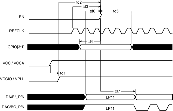 Figure 7-1 Power-Up Timing Definitions for DPPLL_CLK_SRC = REFCLK
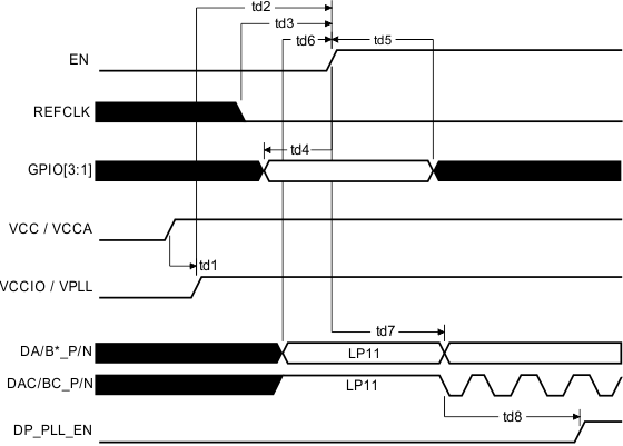 Figure 7-2 Power-Up Timing Definitions for DPPLL_CLK_SRC = DACP/N
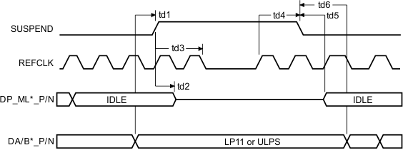 Figure 7-3 SUSPEND Timing Definitions
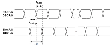 Figure 7-4 DSI HS Mode Receiver Timing Definitions
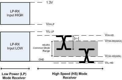 Figure 7-5 DSI Receiver Voltage Definitions