JAJSF58O MARCH   2001  – April 2018 SN65HVD230 , SN65HVD231 , SN65HVD232

PRODUCTION DATA.  

  1. 特長
  2. アプリケーション
  3. 概要
    1.     Device Images
      1.      等価な入力および出力回路図
  4. 改訂履歴
  5. 概要(続き)
  6. Device Comparison Table
  7. Pin Configuration and Functions
    1.     Pin Functions
  8. Specifications
    1. 8.1  Absolute Maximum Ratings
    2. 8.2  ESD Ratings
    3. 8.3  Recommended Operating Conditions
    4. 8.4  Thermal Information
    5. 8.5  Electrical Characteristics: Driver
    6. 8.6  Electrical Characteristics: Receiver
    7. 8.7  Switching Characteristics: Driver
    8. 8.8  Switching Characteristics: Receiver
    9. 8.9  Switching Characteristics: Device
    10. 8.10 Device Control-Pin Characteristics
    11. 8.11 Typical Characteristics
  9. Parameter Measurement Information
  10. 10Detailed Description
    1. 10.1 Overview
    2. 10.2 Functional Block Diagram
    3. 10.3 Feature Description
      1. 10.3.1 Vref Voltage Reference
      2. 10.3.2 Thermal Shutdown
    4. 10.4 Device Functional Modes
      1. 10.4.1 High-Speed Mode
      2. 10.4.2 Slope Control Mode
      3. 10.4.3 Standby Mode (Listen Only Mode) of the HVD230
      4. 10.4.4 The Babbling Idiot Protection of the HVD230
      5. 10.4.5 Sleep Mode of the HVD231
      6. 10.4.6 Summary of Device Operating Modes
  11. 11Application and Implementation
    1. 11.1 Application Information
      1. 11.1.1 CAN Bus States
    2. 11.2 Typical Application
      1. 11.2.1 Design Requirements
        1. 11.2.1.1 CAN Termination
        2. 11.2.1.2 Loop Propagation Delay
        3. 11.2.1.3 Bus Loading, Length and Number of Nodes
      2. 11.2.2 Detailed Design Procedure
        1. 11.2.2.1 Transient Protection
        2. 11.2.2.2 Transient Voltage Suppressors
      3. 11.2.3 Application Curve
    3. 11.3 System Example
      1. 11.3.1 ISO 11898 Compliance of SN65HVD23x Family of 3.3 V CAN Transceivers
        1. 11.3.1.1 Introduction
        2. 11.3.1.2 Differential Signal
          1. 11.3.1.2.1 Common Mode Signal
        3. 11.3.1.3 Interoperability of 3.3-V CAN in 5-V CAN Systems
  12. 12Power Supply Recommendations
  13. 13Layout
    1. 13.1 Layout Guidelines
    2. 13.2 Layout Example
  14. 14デバイスおよびドキュメントのサポート
    1. 14.1 関連リンク
    2. 14.2 ドキュメントの更新通知を受け取る方法
    3. 14.3 コミュニティ・リソース
    4. 14.4 商標
    5. 14.5 静電気放電に関する注意事項
    6. 14.6 Glossary
  15. 15メカニカル、パッケージ、および注文情報

パッケージ・オプション

メカニカル・データ(パッケージ|ピン)
サーマルパッド・メカニカル・データ
発注情報

CAN Bus States

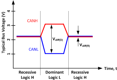
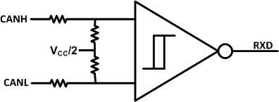
The CAN bus has two states during powered operation of the device; dominant and recessive. A dominant bus state is when the bus is driven differentially, corresponding to a logic low on the D and R pin. A recessive bus state is when the bus is biased to VCC / 2 via the high-resistance internal resistors RI and RDiff of the receiver, corresponding to a logic high on the D and R pins. See Figure 34 and Figure 35.
SN65HVD230 SN65HVD231 SN65HVD232 Fig_1_BusStates_slos346.gifFigure 34. CAN Bus States (Physical Bit Representation)
SN65HVD230 SN65HVD231 SN65HVD232 Fig_2_RecessiveCMbias_slos346.gifFigure 35. Simplified Recessive Common Mode Bias and Receiver