JAJSF58O MARCH   2001  – April 2018 SN65HVD230 , SN65HVD231 , SN65HVD232

PRODUCTION DATA.  

  1. 特長
  2. アプリケーション
  3. 概要
    1.     Device Images
      1.      等価な入力および出力回路図
  4. 改訂履歴
  5. 概要(続き)
  6. Device Comparison Table
  7. Pin Configuration and Functions
    1.     Pin Functions
  8. Specifications
    1. 8.1  Absolute Maximum Ratings
    2. 8.2  ESD Ratings
    3. 8.3  Recommended Operating Conditions
    4. 8.4  Thermal Information
    5. 8.5  Electrical Characteristics: Driver
    6. 8.6  Electrical Characteristics: Receiver
    7. 8.7  Switching Characteristics: Driver
    8. 8.8  Switching Characteristics: Receiver
    9. 8.9  Switching Characteristics: Device
    10. 8.10 Device Control-Pin Characteristics
    11. 8.11 Typical Characteristics
  9. Parameter Measurement Information
  10. 10Detailed Description
    1. 10.1 Overview
    2. 10.2 Functional Block Diagram
    3. 10.3 Feature Description
      1. 10.3.1 Vref Voltage Reference
      2. 10.3.2 Thermal Shutdown
    4. 10.4 Device Functional Modes
      1. 10.4.1 High-Speed Mode
      2. 10.4.2 Slope Control Mode
      3. 10.4.3 Standby Mode (Listen Only Mode) of the HVD230
      4. 10.4.4 The Babbling Idiot Protection of the HVD230
      5. 10.4.5 Sleep Mode of the HVD231
      6. 10.4.6 Summary of Device Operating Modes
  11. 11Application and Implementation
    1. 11.1 Application Information
      1. 11.1.1 CAN Bus States
    2. 11.2 Typical Application
      1. 11.2.1 Design Requirements
        1. 11.2.1.1 CAN Termination
        2. 11.2.1.2 Loop Propagation Delay
        3. 11.2.1.3 Bus Loading, Length and Number of Nodes
      2. 11.2.2 Detailed Design Procedure
        1. 11.2.2.1 Transient Protection
        2. 11.2.2.2 Transient Voltage Suppressors
      3. 11.2.3 Application Curve
    3. 11.3 System Example
      1. 11.3.1 ISO 11898 Compliance of SN65HVD23x Family of 3.3 V CAN Transceivers
        1. 11.3.1.1 Introduction
        2. 11.3.1.2 Differential Signal
          1. 11.3.1.2.1 Common Mode Signal
        3. 11.3.1.3 Interoperability of 3.3-V CAN in 5-V CAN Systems
  12. 12Power Supply Recommendations
  13. 13Layout
    1. 13.1 Layout Guidelines
    2. 13.2 Layout Example
  14. 14デバイスおよびドキュメントのサポート
    1. 14.1 関連リンク
    2. 14.2 ドキュメントの更新通知を受け取る方法
    3. 14.3 コミュニティ・リソース
    4. 14.4 商標
    5. 14.5 静電気放電に関する注意事項
    6. 14.6 Glossary
  15. 15メカニカル、パッケージ、および注文情報

パッケージ・オプション

メカニカル・データ(パッケージ|ピン)
サーマルパッド・メカニカル・データ
発注情報

Typical Application

Figure 36 illustrates a typical application of the SN65HVD23x family. The output of the host µP's CAN controller (TXD) is connected to the transceivers driver input, pin D, and the transceivers receiver output, pin R, is connected to the input of the CAN controller (RXD). The transceiver is attached to the differential bus lines at pins CANH and CANL. Typically, the bus is a twisted pair of wires with a characteristic impedance of 120 Ω, in the standard half-duplex multipoint topology of Figure 37. Each end of the bus is terminated with 120 Ω resistors in compliance with the standard to minimize signal reflections on the bus.
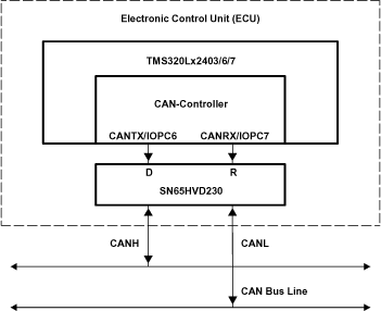
SN65HVD230 SN65HVD231 SN65HVD232 ai_can_node_los346.gifFigure 36. Details of a Typical CAN Node
SN65HVD230 SN65HVD231 SN65HVD232 ai_can_net_los346.gifFigure 37. Typical CAN Network