JAJSF58O MARCH   2001  – April 2018 SN65HVD230 , SN65HVD231 , SN65HVD232

PRODUCTION DATA.  

  1. 特長
  2. アプリケーション
  3. 概要
    1.     Device Images
      1.      等価な入力および出力回路図
  4. 改訂履歴
  5. 概要(続き)
  6. Device Comparison Table
  7. Pin Configuration and Functions
    1.     Pin Functions
  8. Specifications
    1. 8.1  Absolute Maximum Ratings
    2. 8.2  ESD Ratings
    3. 8.3  Recommended Operating Conditions
    4. 8.4  Thermal Information
    5. 8.5  Electrical Characteristics: Driver
    6. 8.6  Electrical Characteristics: Receiver
    7. 8.7  Switching Characteristics: Driver
    8. 8.8  Switching Characteristics: Receiver
    9. 8.9  Switching Characteristics: Device
    10. 8.10 Device Control-Pin Characteristics
    11. 8.11 Typical Characteristics
  9. Parameter Measurement Information
  10. 10Detailed Description
    1. 10.1 Overview
    2. 10.2 Functional Block Diagram
    3. 10.3 Feature Description
      1. 10.3.1 Vref Voltage Reference
      2. 10.3.2 Thermal Shutdown
    4. 10.4 Device Functional Modes
      1. 10.4.1 High-Speed Mode
      2. 10.4.2 Slope Control Mode
      3. 10.4.3 Standby Mode (Listen Only Mode) of the HVD230
      4. 10.4.4 The Babbling Idiot Protection of the HVD230
      5. 10.4.5 Sleep Mode of the HVD231
      6. 10.4.6 Summary of Device Operating Modes
  11. 11Application and Implementation
    1. 11.1 Application Information
      1. 11.1.1 CAN Bus States
    2. 11.2 Typical Application
      1. 11.2.1 Design Requirements
        1. 11.2.1.1 CAN Termination
        2. 11.2.1.2 Loop Propagation Delay
        3. 11.2.1.3 Bus Loading, Length and Number of Nodes
      2. 11.2.2 Detailed Design Procedure
        1. 11.2.2.1 Transient Protection
        2. 11.2.2.2 Transient Voltage Suppressors
      3. 11.2.3 Application Curve
    3. 11.3 System Example
      1. 11.3.1 ISO 11898 Compliance of SN65HVD23x Family of 3.3 V CAN Transceivers
        1. 11.3.1.1 Introduction
        2. 11.3.1.2 Differential Signal
          1. 11.3.1.2.1 Common Mode Signal
        3. 11.3.1.3 Interoperability of 3.3-V CAN in 5-V CAN Systems
  12. 12Power Supply Recommendations
  13. 13Layout
    1. 13.1 Layout Guidelines
    2. 13.2 Layout Example
  14. 14デバイスおよびドキュメントのサポート
    1. 14.1 関連リンク
    2. 14.2 ドキュメントの更新通知を受け取る方法
    3. 14.3 コミュニティ・リソース
    4. 14.4 商標
    5. 14.5 静電気放電に関する注意事項
    6. 14.6 Glossary
  15. 15メカニカル、パッケージ、および注文情報

パッケージ・オプション

メカニカル・データ(パッケージ|ピン)
サーマルパッド・メカニカル・データ
発注情報

Application Curve

Typical driver output waveforms from a pulse input signal with different slope control resistances are displayed in Figure 41. The top waveform show the typical differential signal when transitioning from a recessive level to a dominant level on the CAN bus with RS tied to GND through a zero ohm resistor. The second waveform shows the same signal for the condition with a 10k ohm resistor tied from RS to ground. The bottom waveform shows the typical differential signal for the case where a 100k ohm resistor is tied from the RS pin to ground.
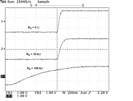
SN65HVD230 SN65HVD231 SN65HVD232 ai_wave2_los346.gifFigure 41. Typical SN65HVD230 250-kbps Output Pulse Waveforms With Slope Control