JAJSPZ4F November 2006 – March 2023 SN65HVD3080E , SN65HVD3083E , SN65HVD3086E
PRODUCTION DATA
- 1 特長
- 2 アプリケーション
- 3 概要
- 4 Revision History
-
5 Specifications
- 5.1 Absolute Maximum Ratings
- 5.2 Power Dissipation Ratings
- 5.3 Electrostatic Discharge Protection
- 5.4 Supply Current
- 5.5 Recommended Operating Conditions
- 5.6 Thermal Information
- 5.7 Driver Electrical Characteristics
- 5.8 Driver Switching Characteristics
- 5.9 Receiver Electrical Characteristics
- 5.10 Receiver Switching Characteristics
- 5.11 Typical Characteristics
- 6 Parameter Measurement Information
- 7 Device Information
- 8 Application Information
- 9 Device and Documentation Support
- 10Mechanical, Packaging, and Orderable Information
パッケージ・オプション
メカニカル・データ(パッケージ|ピン)
サーマルパッド・メカニカル・データ
発注情報
6 Parameter Measurement Information
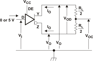
 Figure 6-1 Driver VOD Test Circuit and Current Definitions
 Figure 6-2 Driver VOD With Common-Mode Loading Test Circuit
 Figure 6-3 Test Circuit and Definitions for the Driver Common-Mode Output Voltage
 Figure 6-4 Driver Switching Test Circuit and Voltage Waveforms
 Figure 6-5 Driver High-Level Output Enable and Disable Time Test Circuit and Voltage Waveforms
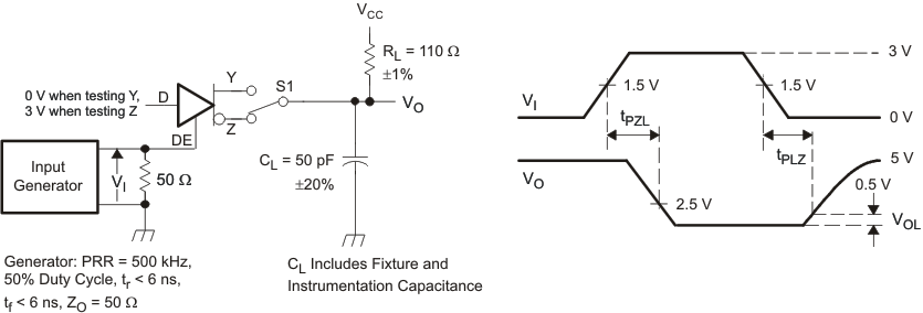
 Figure 6-6 Driver Low-Level Output Enable and Disable Time Test Circuit and Voltage Waveforms
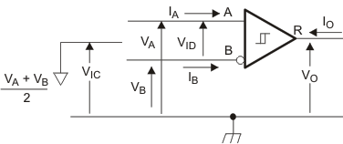
 Figure 6-7 Receiver Voltage and Current Definitions
 Figure 6-8 Receiver Switching Test Circuit and Voltage Waveforms
 Figure 6-9 Receiver Enable and Disable Test Circuit and Voltage Waveforms
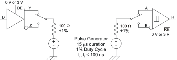
A. This test is conducted to test survivability only. Data stability at the R output is not specified.
Figure 6-10 Transient Overvoltage Test Circuit