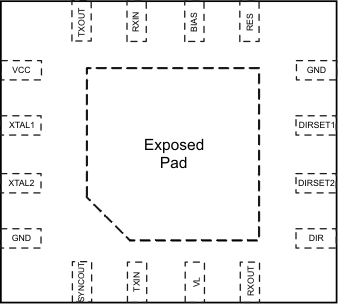
| 1 |
SYNCOUT |
Open drain output to synchronize other devices to the 4x-carrier oscillator at XTAL1,2. (8.704 MHz for HVD62) |
| 2 |
TXIN |
Digital data bit stream to driver. |
| 3 |
VL |
Logic supply voltage for the device. |
| 4 |
RXOUT |
Digital data bit stream from receiver. |
| 5 |
DIR |
DIR: Direction control output signal for bus arbitration.
DIRSET1 and DIRSET2: Bits to set the duration of DIR
DIRSET[2,1]:[L,L]=9.6kbps [L,H]=38.4kbps [H,L]=115kbps [H,H]=Standby Mode |
| 6 |
DIRSET2 |
| 7 |
DIRSET1 |
| 8 |
GND |
Ground |
| 9 |
RES |
Input voltage to adjust driver output power. Set by external resistors from BIAS pin to GND. |
| 10 |
BIAS |
Bias voltage output for setting driver output power by external resistors. |
| 11 |
RXIN |
Modulated input signal to the receiver. |
| 12 |
TXOUT |
Modulated output signal from the driver. |
| 13 |
VCC |
Analog supply voltage for the device. |
| 14 |
XTAL1 |
Crystal oscillator’s IO pins. Connect a 4 x fC crystal between these pins. Or connect XTAL1 to an 8.704 MHz clock and connect XTAL2 to GND. |
| 15 |
XTAL2 |
| 16 |
GND |
Ground |
| - |
EP |
Exposed pad. Recommended to be connected to ground plane for best thermal conduction. |
